Abstract: This applicaTIon note describes techniques of using a PC based Digital I / O Board to characterize analog-to-digital converters (ADCs). It will look at staTIc DC parameters such as integral nonlinearity (INL), differenTIal nonlinearity (DNL), gain, and offset errors, but also noise, internal reference voltage, and channel-to-channel coupling and matching, as well as the supply voltage dependence.
With the increasing complexity of analog-to-digital converters (ADCs), it is becoming more difficult to analyze and characterize these devices in a lab environment. One way to improve the thoroughness of characterizaTIon with ADCs is to use a PC to automate the bench testing. This approach has many advantages, which arise with little additional effort. The most important benefit of using automation in place of manual testing is obtaining a more complete view of the converter's performance much earlier in the characterization process. Also, once the system is in place, designing vectors to debug even complex design errors is usually straightforward.
There are a number of ways a PC can be used to automate characterization of an IC. They range from using a simple parallel-port interface for manipulating control bits, to a closed-loop servo system for fully characterizing all aspects of the device's performance. The following discussion will focus primarily on the approach used to characterize the MAX1115-MAX1119 8-bit successive approximation register (SAR) ADCs. This method is accurate enough to be used for characterizing similar converters with resolutions up to 12 bits. Many of the issues associated with using parallel and serial ports to characterize devices are covered in the article "PCs Provide The Key To Economical Yet Effective Automated Test Systems," published in Electronic Design magazine.
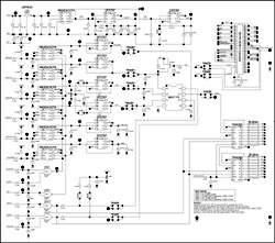
System SetupTo characterize the MAX1115, a high-speed digital I / O card from National Instruments (PCI-DIO-32HS) and a custom characterization board were used. The PCI-DIO-32HS 32-channel digital I / O board can be used to stream vectors to (or from) a PC hard disk from (or to) the custom characterization board at a rate of 20MHz. A schematic of the characterization board is shown below.
For larger image (PDF, 308k)
Figure 1.
The six MAX541s on the left of the schematic are 16-bit serial DACs. They are used to provide the device under test (DUT) VDD supply voltage / reference voltage and the two input signals. In addition, an input-level shifter supply used to adjust the digital input voltage swing into the DUT, and the input-signal DAC reference voltage are provided. The devices immediately to the right of the DACs are OP27 buffer amplifiers. The OP27 is a high-precision op amp that can furnish up to 10mA of drive current for each DAC, with only a slight degradation in the DAC's 16-bit performance. The circuitry on the top of the schematic is input power-supply regulation and conditioning, and the MAX6341, a 4.096V precision voltage reference. On the right side of the schematic are serial-to-parallel shift registers, series terminators, and the PCI-DIO-32HS interface connection.
Static TestingWith static testing, you can control the power supply and reference to the DUT, run various test signals into the DUT, and capture the device's response to these signals with ease. In the case of the MAX1115, all DC accuracy specifications were verified with more precision than was practical to implement in a high-volume production test environment. This was accomplished by using the DUT to measure the ADC input (which actually is the DAC output) several times at each DAC code. With this data, it was not only possible to determine the integral nonlinearity (INL), differential nonlinearity (DNL), gain, and offset errors, but also noise, internal reference voltage, and channel-to-channel coupling and matching, as well as the supply voltage dependence of each of these parameters. A complete set of DC specifications was obtained in a few seconds, which permitted statistical data to be gathered before comparing the data against data obtained from the production test setup. As a result, there was faster identification and resolution of correlation issues between the lab data and test floor data.
Dynamic TestingThe test system developed for the MAX1115 was not intended for verifying dynamic parameters, although such a system can be extended to carry out dynamic testing. To accomplish this, a higher-speed parallel DAC could be used to generate the input signals. It is also possible to have the DAC updated by a circular first-in / first-out (FIFO) memory to generate sine waves (or other repetitive waveforms), with minimal signaling from the PC during the measurement process. Another option is to generate the test signals using an external signal generator.
One nice feature of this type of test system is that a large number of data samples are easily obtained. With dynamic testing, this feature allows for fine frequency resolution and more input test frequencies to be obtained with relative ease, increasing one's confidence in the DUT's characteristics.
AccuracyThe method outlined above is an open-loop characterization scheme and is accurate enough to extend to 10-bit systems. The advantage of this approach is that it is fast. The inherent accuracy and resolution of the characterization board (relative to the DUT) allows for relatively accurate determination of each ADC code center and boundary.
With higher-precision converters (12 bits or more), it may be necessary to design a closed-loop test system. This can be constructed in the same way as outlined above, with the addition of a high-precision digital voltmeter. The digital voltmeter can be interfaced to the same test PC via a general-purpose interface board (GPIB) card, the PC's serial or parallel ports, or an Ethernet connection. The PC is used to step the characterization DACs and find each code boundary in the DUT . Once each code boundary is determined (in DAC codes), the PC then measures the DAC voltage using the high-precision DVM. With a very high resolution DUT, multiple DACs (scaled in resolution to each other) could be used to increase the accuracy of the DUT code boundary measurement.
SpeedAlthough the open-loop test system outlined above was used for a relatively slow speed converter (100ksps), it is directly applicable to higher-speed ADCs. With the addition of on-board logic (perhaps even a field programmable gate array) and an on-board clock, it is possible to provide the signaling necessary to capture data from a 16-bit ADC (serial or parallel) at 20Msps with the National PCI-DIO-32HS interface board. This would require a high-speed parallel test DAC and perhaps a circular FIFO memory to load repetitive test waveforms as discussed above.
Design-Error IdentificationIn cases where design errors need to be identified and corrected, this rapid bench characterization allows for a controlled, iterative evaluation loop (that is, hypothesis, experimental design, measurement and evaluation of results, leading to further hypothesis, experimental design, etc.) and consequently faster identification of the design error. It is conceivable that even complex errors could be identified in a matter of days instead of weeks or months when compared to a more manual approach.
Problems with PC-Based Characterization Systems Often the most significant problems with a PC-based characterization system are signal integrity and common supply noise. Once understood, these problems can be mitigated and in some instances eliminated altogether.
Signal integrity is a result of having too few grounds and too high parasitics in the cabling system. The result is large overshoots and undershoots in the waveform at both ends of the cable. There are a number of approaches that can be used to reduce the magnitude of this problem. One of the simplest methods is to use series termination. In this scheme, a series resistor (RT) roughly equal to the characteristic impedance (Z0) of the interconnecting cable (minus the source driver impedance, ZD) is placed at the source end of the cable shown in Figure 2. The parasitic capacitance of the cable will in effect turn the circuit into a first-order-dominated system with a somewhat slower rise time at the badly matched receiver end. With this scheme, the badly matched receiver reflects rapid transitioning edges back to the source side of the circuit, where they are absorbed, because of its proper termination.
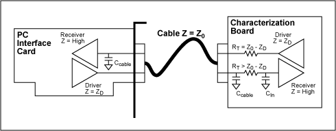
Figure 2.
This approach works well for signals traveling from the characterization board to the PC interface card, because terminating resistors can be placed at the source end of the characterization board. However, with signals traveling from the PC interface card to the characterization board, it is not Possible to add these terminating resistors on the PC interface card. Thus, it is often necessary to overcompensate by using larger series termination resistance and adding more input capacitance following the termination resistor to achieve acceptable results (Figure 2). Adding sockets where DIP termination resistor arrays can be changed allows the value of the series termination resistor to be varied, depending on the cable length and the driver / receiver combinations used.
Another approach for improving receiver-end signal integrity on the characterization board is using shunt termination. In this scheme, shown in Figure 3, rapid edges from the interface board are absorbed in a properly matched shunt termination. Because this method reduces signal swing (the driver impedance in the interface card is significant), it is necessary to use a termination power supply to adjust the incoming signal levels to acceptable logic levels for the input receiver. This loss in signal swing, continuous power dissipation, and increased ground current in the cable are all significant disadvantages of this approach. AC shunt termination, where the termination power supply is replaced with a capacitor, solves these problems but results in the well-known predicament of a metastable state during level transitions and therefore is not recommended.
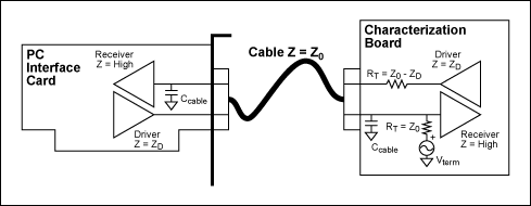
Figure 3.
Common supply noise, the second major problem, occurs because the noisy PC ground injects noise current through the characterization board into the characterization bench supply and the oscilloscope ground. This injected noise current can generate significant voltage drop (several LSBs) across the characterization board ground , which can be coupled into the input of the converter.
One solution to this problem is to use multiple, continuous ground planes (connected through numerous vias) in the characterization board to reduce its impedance and thus the voltage drop. Isolating ground planes tends to be less effective because of the inevitable capacitive coupling between isolated ground planes and the fact that typical noise current injected from PCs is high in frequency, effectively shorting the isolated ground planes. Increasing the isolation (from earth ground) in the bench supplies used to power the characterization board can also help. It is recommended that oscilloscope probes be removed (grounds included) when collecting data from the DUT, to eliminate ground currents from the PC to the oscilloscope probe grounds. Another solution is to have local power regulation and conditioning on the characterization board. It may be necessary to perform experiments to isolate and eliminate the cause of common-mode noise while debugging the characterization system.
ConclusionThe bench characterization of the MAX1115, an 8-bit ADC using a low-cost PC-based data-acquisition system, has proven to be effective and accurate. A number of advantages of this approach to bench characterization have been pointed out and include ease of interfacing to complex devices, more complete and faster characterization of both static and dynamic parameters, the ability to improve design-error identification, and faster resolution of correlation issues. Although the approach outline is directly applicable to ADCs with resolutions up to 12 bits and speeds of up to about 500ksps, the means of extending this test method both in resolution and speed have been discussed.
With the increasing complexity of analog-to-digital converters (ADCs), it is becoming more difficult to analyze and characterize these devices in a lab environment. One way to improve the thoroughness of characterizaTIon with ADCs is to use a PC to automate the bench testing. This approach has many advantages, which arise with little additional effort. The most important benefit of using automation in place of manual testing is obtaining a more complete view of the converter's performance much earlier in the characterization process. Also, once the system is in place, designing vectors to debug even complex design errors is usually straightforward.
There are a number of ways a PC can be used to automate characterization of an IC. They range from using a simple parallel-port interface for manipulating control bits, to a closed-loop servo system for fully characterizing all aspects of the device's performance. The following discussion will focus primarily on the approach used to characterize the MAX1115-MAX1119 8-bit successive approximation register (SAR) ADCs. This method is accurate enough to be used for characterizing similar converters with resolutions up to 12 bits. Many of the issues associated with using parallel and serial ports to characterize devices are covered in the article "PCs Provide The Key To Economical Yet Effective Automated Test Systems," published in Electronic Design magazine.
System SetupTo characterize the MAX1115, a high-speed digital I / O card from National Instruments (PCI-DIO-32HS) and a custom characterization board were used. The PCI-DIO-32HS 32-channel digital I / O board can be used to stream vectors to (or from) a PC hard disk from (or to) the custom characterization board at a rate of 20MHz. A schematic of the characterization board is shown below.

For larger image (PDF, 308k)
Figure 1.
The six MAX541s on the left of the schematic are 16-bit serial DACs. They are used to provide the device under test (DUT) VDD supply voltage / reference voltage and the two input signals. In addition, an input-level shifter supply used to adjust the digital input voltage swing into the DUT, and the input-signal DAC reference voltage are provided. The devices immediately to the right of the DACs are OP27 buffer amplifiers. The OP27 is a high-precision op amp that can furnish up to 10mA of drive current for each DAC, with only a slight degradation in the DAC's 16-bit performance. The circuitry on the top of the schematic is input power-supply regulation and conditioning, and the MAX6341, a 4.096V precision voltage reference. On the right side of the schematic are serial-to-parallel shift registers, series terminators, and the PCI-DIO-32HS interface connection.
Static TestingWith static testing, you can control the power supply and reference to the DUT, run various test signals into the DUT, and capture the device's response to these signals with ease. In the case of the MAX1115, all DC accuracy specifications were verified with more precision than was practical to implement in a high-volume production test environment. This was accomplished by using the DUT to measure the ADC input (which actually is the DAC output) several times at each DAC code. With this data, it was not only possible to determine the integral nonlinearity (INL), differential nonlinearity (DNL), gain, and offset errors, but also noise, internal reference voltage, and channel-to-channel coupling and matching, as well as the supply voltage dependence of each of these parameters. A complete set of DC specifications was obtained in a few seconds, which permitted statistical data to be gathered before comparing the data against data obtained from the production test setup. As a result, there was faster identification and resolution of correlation issues between the lab data and test floor data.
Dynamic TestingThe test system developed for the MAX1115 was not intended for verifying dynamic parameters, although such a system can be extended to carry out dynamic testing. To accomplish this, a higher-speed parallel DAC could be used to generate the input signals. It is also possible to have the DAC updated by a circular first-in / first-out (FIFO) memory to generate sine waves (or other repetitive waveforms), with minimal signaling from the PC during the measurement process. Another option is to generate the test signals using an external signal generator.
One nice feature of this type of test system is that a large number of data samples are easily obtained. With dynamic testing, this feature allows for fine frequency resolution and more input test frequencies to be obtained with relative ease, increasing one's confidence in the DUT's characteristics.
AccuracyThe method outlined above is an open-loop characterization scheme and is accurate enough to extend to 10-bit systems. The advantage of this approach is that it is fast. The inherent accuracy and resolution of the characterization board (relative to the DUT) allows for relatively accurate determination of each ADC code center and boundary.
With higher-precision converters (12 bits or more), it may be necessary to design a closed-loop test system. This can be constructed in the same way as outlined above, with the addition of a high-precision digital voltmeter. The digital voltmeter can be interfaced to the same test PC via a general-purpose interface board (GPIB) card, the PC's serial or parallel ports, or an Ethernet connection. The PC is used to step the characterization DACs and find each code boundary in the DUT . Once each code boundary is determined (in DAC codes), the PC then measures the DAC voltage using the high-precision DVM. With a very high resolution DUT, multiple DACs (scaled in resolution to each other) could be used to increase the accuracy of the DUT code boundary measurement.
SpeedAlthough the open-loop test system outlined above was used for a relatively slow speed converter (100ksps), it is directly applicable to higher-speed ADCs. With the addition of on-board logic (perhaps even a field programmable gate array) and an on-board clock, it is possible to provide the signaling necessary to capture data from a 16-bit ADC (serial or parallel) at 20Msps with the National PCI-DIO-32HS interface board. This would require a high-speed parallel test DAC and perhaps a circular FIFO memory to load repetitive test waveforms as discussed above.
Design-Error IdentificationIn cases where design errors need to be identified and corrected, this rapid bench characterization allows for a controlled, iterative evaluation loop (that is, hypothesis, experimental design, measurement and evaluation of results, leading to further hypothesis, experimental design, etc.) and consequently faster identification of the design error. It is conceivable that even complex errors could be identified in a matter of days instead of weeks or months when compared to a more manual approach.
Problems with PC-Based Characterization Systems Often the most significant problems with a PC-based characterization system are signal integrity and common supply noise. Once understood, these problems can be mitigated and in some instances eliminated altogether.
Signal integrity is a result of having too few grounds and too high parasitics in the cabling system. The result is large overshoots and undershoots in the waveform at both ends of the cable. There are a number of approaches that can be used to reduce the magnitude of this problem. One of the simplest methods is to use series termination. In this scheme, a series resistor (RT) roughly equal to the characteristic impedance (Z0) of the interconnecting cable (minus the source driver impedance, ZD) is placed at the source end of the cable shown in Figure 2. The parasitic capacitance of the cable will in effect turn the circuit into a first-order-dominated system with a somewhat slower rise time at the badly matched receiver end. With this scheme, the badly matched receiver reflects rapid transitioning edges back to the source side of the circuit, where they are absorbed, because of its proper termination.

Figure 2.
This approach works well for signals traveling from the characterization board to the PC interface card, because terminating resistors can be placed at the source end of the characterization board. However, with signals traveling from the PC interface card to the characterization board, it is not Possible to add these terminating resistors on the PC interface card. Thus, it is often necessary to overcompensate by using larger series termination resistance and adding more input capacitance following the termination resistor to achieve acceptable results (Figure 2). Adding sockets where DIP termination resistor arrays can be changed allows the value of the series termination resistor to be varied, depending on the cable length and the driver / receiver combinations used.
Another approach for improving receiver-end signal integrity on the characterization board is using shunt termination. In this scheme, shown in Figure 3, rapid edges from the interface board are absorbed in a properly matched shunt termination. Because this method reduces signal swing (the driver impedance in the interface card is significant), it is necessary to use a termination power supply to adjust the incoming signal levels to acceptable logic levels for the input receiver. This loss in signal swing, continuous power dissipation, and increased ground current in the cable are all significant disadvantages of this approach. AC shunt termination, where the termination power supply is replaced with a capacitor, solves these problems but results in the well-known predicament of a metastable state during level transitions and therefore is not recommended.

Figure 3.
Common supply noise, the second major problem, occurs because the noisy PC ground injects noise current through the characterization board into the characterization bench supply and the oscilloscope ground. This injected noise current can generate significant voltage drop (several LSBs) across the characterization board ground , which can be coupled into the input of the converter.
One solution to this problem is to use multiple, continuous ground planes (connected through numerous vias) in the characterization board to reduce its impedance and thus the voltage drop. Isolating ground planes tends to be less effective because of the inevitable capacitive coupling between isolated ground planes and the fact that typical noise current injected from PCs is high in frequency, effectively shorting the isolated ground planes. Increasing the isolation (from earth ground) in the bench supplies used to power the characterization board can also help. It is recommended that oscilloscope probes be removed (grounds included) when collecting data from the DUT, to eliminate ground currents from the PC to the oscilloscope probe grounds. Another solution is to have local power regulation and conditioning on the characterization board. It may be necessary to perform experiments to isolate and eliminate the cause of common-mode noise while debugging the characterization system.
ConclusionThe bench characterization of the MAX1115, an 8-bit ADC using a low-cost PC-based data-acquisition system, has proven to be effective and accurate. A number of advantages of this approach to bench characterization have been pointed out and include ease of interfacing to complex devices, more complete and faster characterization of both static and dynamic parameters, the ability to improve design-error identification, and faster resolution of correlation issues. Although the approach outline is directly applicable to ADCs with resolutions up to 12 bits and speeds of up to about 500ksps, the means of extending this test method both in resolution and speed have been discussed.
Dj Speaker,Portable Bluetooth Speaker,Lf600 Multifunctional Speaker,Speakers For Large Events
NINGBO RFUN AUDIO TECHNOLOGY CO.,LTD , https://www.mosensound.com