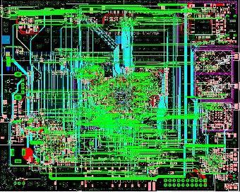
PCB package is actually to display components, chips and other parameters (such as size, length and width, pad size, etc.) in a graphical manner, so that it can be called when drawing a PCB. Therefore, before the PCB design, the choice of components becomes a top priority. Otherwise, you will always encounter such problems in the design process. As a result, PCB boards that you spent a lot of time designing can never be used in practice. Today, we will introduce some points for you when choosing PCB components.
The main point here is to explain the techniques of parsing the selection components from the PCB design package. The component package contains a lot of information, including the dimensions of the component, especially the relative position of the pins, and the pad type of the component. Of course, one of the things we should pay attention to when selecting components based on component packaging is to consider the component's external dimensions.

The pin position relationship: mainly means that we need to match the actual component's pin to the PCB's package size. We choose different components, although the function is the same, but the component package is likely to be different. We need to ensure that the PCB pad is in the correct position to ensure that the component is properly soldered.
Pad selection: This is where we need to consider more.
Yuankun Zhizao's main businesses are component sales, PCB BOARD, SMT welding, layout design, BOM quotes, the company has strong technical strength, perfect detection means, with the most direct supply channels, is the agent of many famous companies in the world.
First include the type of pad. The type includes two kinds, one is the plated through hole, one is the surface mount type. Factors that we need to consider include device cost, availability, device area density, and power consumption. From a manufacturing perspective, surface-mount devices are generally less expensive than through-hole devices, and generally have higher availability. For our general design, we chose surface mount components that not only facilitate manual soldering, but also facilitate better connection pads and signals during troubleshooting and debugging.
Second, we should also pay attention to the location of the pad. Because of the different locations, it represents the actual location of the components. If we do not reasonably arrange the position of the pad, it is very likely that there will be a situation where one zone element is too dense and the other zone element is sparse. Of course, the situation is even worse because the pad is located too close to the gap between the elements. Too small to be soldered, the following is an example of my failure. I opened a via next to an optocoupler switch, but due to their close proximity, the optocoupler switch can no longer be screwed after the optocoupler switch is soldered on.
Another situation is that we have to consider how the pads are soldered. In the actual process, we often arrange the pads in a specific direction, which is more convenient for welding.
Component Dimensions: In practice, some components (such as polar capacitors) may have high headroom restrictions, so we need to consider them during component selection. When we first started designing, we could draw a basic circuit board shape and place some large or position-critical components (such as connectors) that we plan to use. In this way, you can visually and quickly see (without routing) board virtual perspectives, and give relatively accurate board and component relative positioning and component height. This will help ensure that the PCB is properly placed in the outer packaging (plastics, chassis, chassis, etc.) after assembly. Of course, we can also call the 3D preview mode from the Tools menu to browse the whole board.
For the selection of components, in addition to design requirements, we must also select the products produced by regular manufacturers, so as to ensure the realization of your design goals.
Round Hole Breadboard,Solderless Breadboard Connections,Tie Point Breadboard,Solderless Prototype Breadboard
Cixi Zhongyi Electronics Factory , https://www.zybreadboard.com