Introduction
Today's electronics are no longer the same as TVs and refrigerators of the 1970s, and consumers are updated every few decades. Nowadays, every member of every family is a consumer of electronic products, and as technology continues to bring a variety of new features that people can afford for smart phones, tablets, cars and television, people buy new ones every year. product.
One of the common features of these electronic products is the use of wireless technology, which is highly dependent on RF RF circuits. Unfortunately, even the most confident designers are often discouraged with RF circuits because of the enormous design challenges and the need for specialized design and analysis tools. Because of this, the RF portion of the PCB has been designed by independent designers with RF design expertise for many years.
Why is it so difficult to design RF and microwave PCB designs?
There are many problems in the design process and can have a serious impact on quality and productivity. For example, when embedding a designer's RF circuitry into other designers' PCBs, efficiency is bound to be compromised because they often use different design formats. In addition, designers are often forced to make changes in their designs to work with RF circuits. Since simulations are often performed in RF circuits, rather than in the context of the entire PCB, the significant impact of the board on the RF circuitry may be missed, and vice versa.
As RF content continues to increase, PCB designers and engineers realize that to improve productivity and product quality, it is best for them to address their own RF design challenges within their own design tools. Unfortunately, most desktop PCB design tools don't help them simplify this task.
For example, after modeling a circuit using an RF simulator, once the desired electrical performance is achieved, the simulator produces the copper foil shape of the circuit (usually in DXF format) for import into the PCB design tool. This process often causes some confusion for the designer, for example, the DXF file cannot be converted correctly and cannot be converted into a copper foil shape. In this case, the designer needs to manually import the DXF file, which may cause human error and error in the shape and size, resulting in failure of the RF circuit.
The challenges faced by PCB designers or engineers in trying to design Layouts for RF and microwave circuits are far more than just the above. However, fortunately, there are small solutions in your design tools that can play an important role in resolving these challenges. This white paper will introduce you to six tips to help you simplify any RF PCB design tasks and reduce stress!
1. Maintain a good, accurate RF shape
Some serious errors like the one described above can cause poor circuit performance or even work. To minimize errors, simplify RF design tasks, and increase productivity, PCB design tools provide import control for complex copper foil shapes. For example, you can create a usable copper foil shape by controlling the layers in the DXF file and re-imaging them into the CAD electrical system layer (Figure 1).

Figure 1: Design tools that allow users to control the DXF import process will help reduce human error and errors, such as when imported files cannot be converted to copper foil shapes due to high complexity.
2. Keep the corner shape (CORNERS SHARP)
When designing copper foil shapes for RF and microwave, an important aspect is the ability to create Gerber files with sharp corners. Excellent PCB design tools can simplify this process. For example, drawing a shape with a 50 mm line tends to have a smaller radius than a 50 mm circular aperture drawing. When designing a Gerber file, the design tool can obtain a sharp corner by correctly converting the line width automatically (Figure 2).
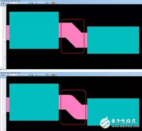
Figure 2: An effective PCB design tool automatically considers the line shape used to draw shapes to calculate the exact line width, helping you easily create sharp corners.
Bitmain Miner:Bitmain Antminer L7 (9.5Gh),Bitmain Antminer L7 (9.16Gh),Bitmain Antminer L7 (9.05Gh),Bitmain Antminer L3+ (504Mh),Bitmain Antminer L3+ (600Mh),Bitmain Antminer L3++ (580Mh),Bitmain Antminer L3++ (596Mh)
Bitmain is the world's leading digital currency mining machine manufacturer. Its brand ANTMINER has maintained a long-term technological and market dominance in the industry, with customers covering more than 100 countries and regions. The company has subsidiaries in China, the United States, Singapore, Malaysia, Kazakhstan and other places.
Bitmain has a unique computing power efficiency ratio technology to provide the global blockchain network with outstanding computing power infrastructure and solutions. Since its establishment in 2013, ANTMINER BTC mining machine single computing power has increased by three orders of magnitude, while computing power efficiency ratio has decreased by two orders of magnitude. Bitmain's vision is to make the digital world a better place for mankind.
Bitmain Miner,antminer L3 Miner,Asic L3 Antminer,Bitmain Antminer L7,ltc miner
Shenzhen YLHM Technology Co., Ltd. , https://www.hkcryptominer.com