Chemical vapor deposition (CVD) can produce materials with the advantages of high quality, high purity, and high strength, and is therefore very popular in the semiconductor industry. Ultra High Vacuum Chemical Vapor Deposition (UHV/CVD) involves fairly complex equipment and extremely high temperatures. Engineers can simulate this complex process in order to better control costs while increasing efficiency. In this article, we will illustrate the growth of silicon substrates as an example.
What is UHV/CVD?
In the CVD process, in the chemical process, a reaction or decomposition occurs on the surface of the exposed substrate to produce a deposited film or film. We generally use CVD to produce materials with higher quality and strength, such as graphene, a powerful and unique material that continues to occupy the headlines of science. CVD can also be used to produce a variety of general-purpose products, from carbon nanofibers to synthetic diamonds, and so is highly valued. In semiconductor applications, high-purity silicon epitaxial layers can be grown using CVD.

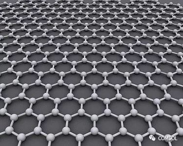
Graphene is one of the materials that can be produced by UHV/CVD. Image courtesy of AlexanderAlUS. Licensed for Creative Commons Attribution-Share Alike 3.0 Unported and shared via Wikimedia Commons.
The UHV/CVD process needs to operate at pressures below 10-6 Pa (approximately 10-8 torr). The process uses molecular streams to deliver gases. UHV/CVD does not involve hydrodynamic effects such as boundary layers; furthermore, gas phase chemistry is not involved because of the low frequency of molecular collisions. The growth rate of a material on a substrate generally depends on the molecular flux of the material reaching the surface. We can also produce graphene with the UHV/CVD process, which we discussed in the fourth part of the Graphene Revolution series.
Utilize COMSOL Multiphysics® Software to Simulate UHV/CVD
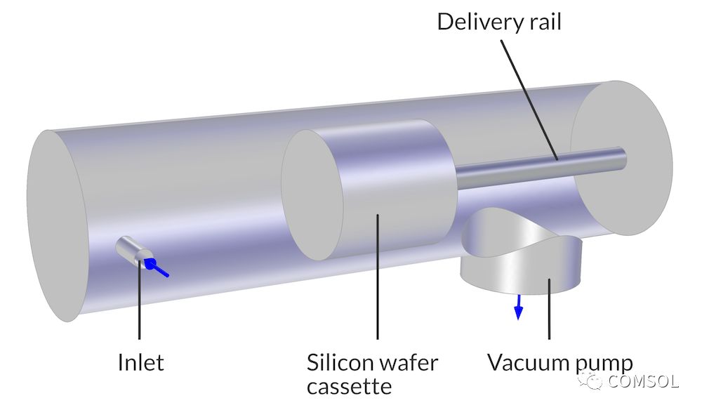
As mentioned earlier, UHV/CVD experiments are often time consuming, expensive, and require special materials and complicated thermal management. Fortunately, we can use the free molecular flow interface in the molecular flow module (one of the add-on modules of the COMSOL Multiphysics simulation platform) to simulate this chemical process. In the model, the substrates are closely arranged on a moving hull inside a quartz tube that is surrounded by a boiler. The wafer cassette is placed in the pipe through the transfer rail.
The reaction gas and ballast gas are locked into the reaction chamber through a pre-vacuum at one end. The turbo pump is located at the other end of the reaction chamber.

Model geometry of the reaction chamber used in the UHV/CVD process.
In the simulation, the reaction gas silane and the ballast gas hydrogen enter from the system inlet at a standard mass flow rate of 1 SCCM, and the ratio of silane to hydrogen is 20%:80%. The entrance of the reaction chamber was set as the exhaust wall boundary condition. A vacuum pump is placed in the cylindrical port at the other end of the reaction chamber.
Simulation allows us to analyze this process for each pump speed profile. We analyzed three different silane and hydrogen pump speed curves and entered these curves into the COMSOL Multiphysics software as an interpolation function. After that, we can use parametric sweeps to analyze the transmission of various gases under different pump speed curves.
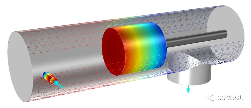
In the bottom surface diagram, we can see the growth of silicon on the substrate under one of the pump speed curves.

The fraction of silane flux in the wafer stack, which controls the growth on the substrate.
The molecular flux fraction of silane on the surface of the substrate (0.04) is much lower than the inlet (0.2). The molecular weight of hydrogen is lower, so pumping is more difficult than silane. Since this measurement directly controls the amount of growth on the substrate, the choice of silane pump and hydrogen pump has a significant effect on the amount of material produced by UHV/CVD. Since it is difficult to measure the molecular flux fraction of each material through physical experiments, simulations can be used to analyze and optimize the UHV/CVD process.

A solar cell panel, solar electric panel, photo-voltaic (PV) module, PV panel or Solar Panel is an assembly of photovoltaic solar cells mounted in a (usually rectangular) frame, and a neatly organised collection of PV panels is called a photovoltaic system or solar array. Solar panels capture sunlight as a source of radiant energy, which is converted into electric energy in the form of direct current (DC) electricity.
60w Solar Panel,Solar Panel System For Home,Solar Panels 200 Watt,Solar Panels
suzhou whaylan new energy technology co., ltd , https://www.whaylan.com