Some people say that the era of human eyes is past, and the era of machine vision is coming. When a reporter asked Yi Jihui, vice president of global market and application engineering of ON Semiconductor's image sensor department, whether he agreed with this view, he replied, “Whether the era of human-eye vision has become a thing of the past remains to be discussed, but it is artificial With the advancement of smart development and application, the wide application of machine vision is undoubtedly accelerated."
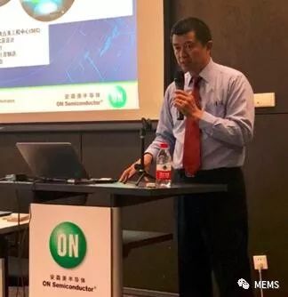
Yi Jihui, vice president of global market and application engineering of ON Semiconductor's image sensor division, creates new vision that exceeds the human eye. This is the new definition of the mission of ON Semiconductor's image sensor department, but how to make this mission from Slogans become reality? It has become a difficult problem facing Yi Jihui. “The key to creating imaging that goes beyond the human eye is continuous innovation.†He told reporters that the human eye is one of the most complex and sophisticated organs in the human body, so creating vision beyond the human eye is a challenge And the complicated process requires us to innovate in many areas such as design, materials, manufacturing processes, image signal processing, and optics.
The advantages of ON Semiconductor are not only the DNA of independent innovation, but also create many products and technologies pioneered by the industry, and have accumulated the industry's largest intellectual property portfolio, plus the reserves of the world's top engineering talent and partners with customers and ecosystems. The close cooperation allows the company to continue to invest in innovation and continue to develop future technologies. On the other hand, as AI has a wide-ranging impact on the future of human life and work, the current trend is that the demand for "edge AI" or "terminal AI" is increasing, for smart cameras and smart vision. The demand is increasing. Yi Jihui expects that in the imaging business, AI will greatly influence the current way of designing and manufacturing image sensors, and change the way it designs and builds imaging solutions, making intelligent imaging and adaptive imaging solutions a new frontier for innovation. In adaptive imaging, for example, image sensors will be able to capture and provide image information that is only useful and important for AI algorithms. At the same time, accelerating the adoption of multi-wafer stacking will become a new trend. Wafer stacking will make it possible to highly integrate various capabilities such as image acquisition, signal processing, image sensing, and object recognition in smart terminal devices.
The era of machine vision is approaching In general, today's imaging products have two broad categories of applications: viewing and sensing. Vision refers to the human eye vision, that is, the captured images (pictures and videos) are mainly used for human eyes to see and comprehend; sensing refers to machine vision, that is, images taken for algorithm or machine learning comprehension.
In other words, in human eyes, images are seen and appreciated by the human eye. Therefore, images usually need to be clear, detailed, colorful, and beautiful. In machine vision, images need to provide enough information, such as edges, shapes, sizes, etc., to be read and understood by the algorithm. “There is no distinction between human vision and machine vision because they serve different purposes and applications. In the past, human eye vision dominated imaging applications and development, with the development of artificial intelligence and the development of smart edge devices. With strong demand, we expect more technology and product innovations in machine vision applications,†Yi Jihui said. Machine vision applications are very extensive and diverse, covering a range of market segments including electronics manufacturing, flat panel inspection, robotics, logistics, and more. At present, China has become the fastest growing country in the global machine vision market. With the implementation of the Chinese-made 2025 plan, China is trying to change the image of low-cost manufacturing plants and establish its reputation as a brand of high-quality and innovative products.
How to build a strong corporate culture and commitment based on high quality and innovation is becoming a challenge and an opportunity for Chinese companies. According to Yi Jihui's introduction, in order to be able to capture clear images of moving objects, the global shutter technology has become the basic requirement of the machine vision market, and its efficiency is one of the key performance indicators. For example, in flat panel inspection applications, the demand for higher resolution, better image uniformity, and higher shutter speeds continues to increase, driven mainly by higher panel resolution (4K and 8K) and increased productivity. In order to support these needs, high-performance small pixel technology is critical; in robotics and electronics manufacturing applications, smart cameras and smart vision are also becoming important drivers. In the industrial sector, ON Semiconductor has launched two new X-Class platforms, including the XGS 8000 with 4K Ultra High Definition (4096 x 2180) resolution and the XGS 12000 with 12 million pixels (4096 x 3072) resolution.
The package size of both devices combined with low heat dissipation is a result of the low voltage, low power architecture of the X-Class interface and is fully compatible with the compact 29x29 mm2 camera design. XGS 12000 and XGS 8000 will begin sampling in the second quarter of 2018 and plan to mass production in the third quarter. Both devices are available in monochrome and color-configured 163-lead LGA packages. The future X-Class family will also include devices based on 3.2 um XGS pixels and products based on other pixel architectures.
No single technology can be applied to all applications Due to the rapid development of in-vehicle applications, machine vision, face recognition and security monitoring, and more and more powerful mobile camera functions (such as dual cameras or three cameras), the sales of global CMOS image sensors have been repeated With high innovations, IC Insights, a market research organization, reported sales of US$ 12.5 billion in 2017, a year-on-year increase of 19%. It is expected that sales of CMOS image sensors will reach US$ 13.7 billion in 2018, an increase of 10% year-on-year. It will record a record for eight consecutive years. . Looking further back, the agency believes that until 2022, CMOS image sensors will maintain a record high in both shipment volume and sales year after year.
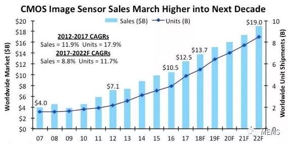
IC Insights pointed out in its latest report that the application of CMOS image sensors has been continuously expanding, emerging applications have continued to emerge, and they have been encroaching on the market share of CCDs (charge-coupled devices). As the smart phone market matures, only 6% of CMOS image sensors grew in 2016. However, the market for non-mobile phone applications soared. As a result, the CMOS sensor market increased by 19% year-on-year in 2017. By comparison, CCD is extremely bleak and 2016 is still growing. 5%, but in 2017 it fell by 2%, with sales of US$1.6 billion. ON Semiconductor has layouts in both CCD and CMOS image sensor technology. In Yi Jihui's view, CMOS has in fact replaced CCDs as the mainstream technology for low- and medium-resolution applications. However, he also reminded the industry that there are currently misunderstandings in the market that CMOS technology is suitable for all applications and that artificially developing products and applications that are not suitable for CMOS technology is absolutely wrong.
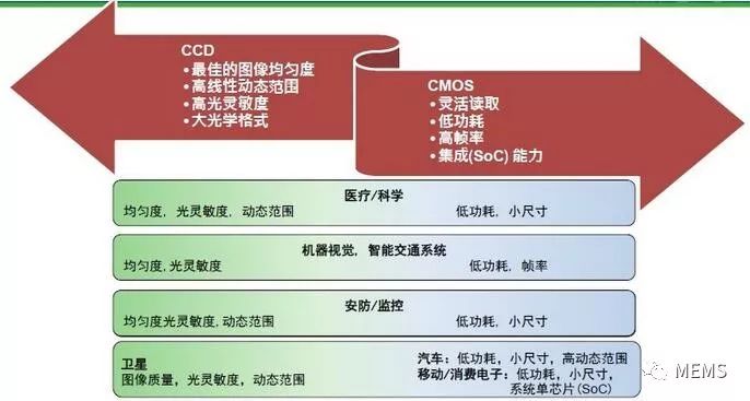
No single technology can be applied to all applications "CCD technology still has a high competitive advantage in some applications. For example, in applications where high image performance and high resolution are critical, we see that CCD has advantages and strong demand. "The first case of application of CCD technology enumerated by Yi Jihui came from the detection of 4K/8K displays, and the other from the EMCCD. This CCD technology can provide ultra-high sensitivity in extremely low light conditions, and this is exactly the CMOS Technology is difficult to achieve. Therefore, he believes that in order to achieve market success and provide end-customers with the most optimized products and services, it is important to carefully select appropriate technologies that can provide tailor-made optimization solutions for specific applications rather than adopting a one-size-fits-all approach. the way. Complete layout of the three major areas of the United States Semiconductor image sensors are mainly concentrated in the industrial, consumer and automotive three major areas. In general, all imaging applications share many common trends and requirements, such as better imaging performance, lower cost, lower power consumption, etc., but each market segment will have some more based on its unique applications. Specific requirements.
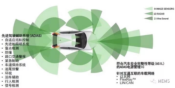
In the automotive market, with the increasing demand for ADAS and automatic driving, high dynamic range (HDR) and low light sensitivity have become very important because cameras are expected to work under all environmental conditions such as direct sunlight and nighttime In the absence of streetlights, as more and more traffic lights and traffic signs are equipped with LED lights, the elimination of LED flicker (LFM) has become a basic requirement for automotive image sensors; in the field of industrial automation and machine vision, the With the clear image of fast moving objects, global shutters have become an important requirement; in consumer and especially Internet of Things applications, ultra-low power consumption has become an important differentiator for battery-powered applications. In addition, ON Semiconductor is the first company in the industry to offer a lineup of image sensor products with functional security and network security capabilities. The industrial market layout has been described previously. Here, we will focus on the automotive and consumer markets.
New automotive CMOS image sensors are continuously improving in terms of photometric level, camera speed and resolution, and integrate more for applications such as security monitoring, machine vision, face recognition, gesture interaction, virtual and augmented reality, and medical systems Dedicated functionality has become an indisputable fact. IC Insights predicts that in the next five years, automotive applications will be the fastest growing direction in the major application markets for CMOS image sensors. In 2022, sales of automotive CMOS image sensors will reach US$2.8 billion, with a compound annual growth rate of 38.4%. More than a decade ago, ON Semiconductor developed the world's first automotive image sensor, currently shipping more than 300 million units in total, supporting a full range of applications including rear-view, look-around, fatigue monitoring, electronic rearview mirrors, ADAS and autonomous driving. Automotive applications. Data shows that ON Semiconductor has a 51% share of the global automotive image sensor market, and ADAS uses image sensors to account for 70% of the global market.
However, their "ambition" is obviously more than that. How to use sensors such as image sensors, radar, LiDAR, and ultrasonic sensors in the field of autopilot, and how to become the leading supplier of automotive autopilot sensors solutions? It is the goal of ON Semiconductor. To this end, ON Semiconductor acquired the IBM Radar Design Center in Israel in 2017 and plans to launch samples using radar technology in the second half of this year. In May of this year, it acquired the silicon photomultiplier tube (SiPM) and single photon avalanche diode ( SPAD) and SensL Technologies Ltd, supplier of LiDAR Sensing Products, meet the needs of LiDAR and sensor fusion in automotive autopilot, robotics, and medical imaging.
The demand for image sensors in the unmanned shops, sales terminals, and logistics fields of the ON Semiconductor Autonomous Driving Program is increasing. The Amazon Image Sensors are found in Amazon's unmanned shops, mobile robot racks, and robot logistics systems. Among them, 8 cameras on every shelf of the Amazon GO unattended store are all from ON Semiconductor; Wal-Mart uses robots to automatically scan the shelves and monitor the out-of-shelf condition of the shelves. Each robot is equipped with 15 ONSOME image sensors.
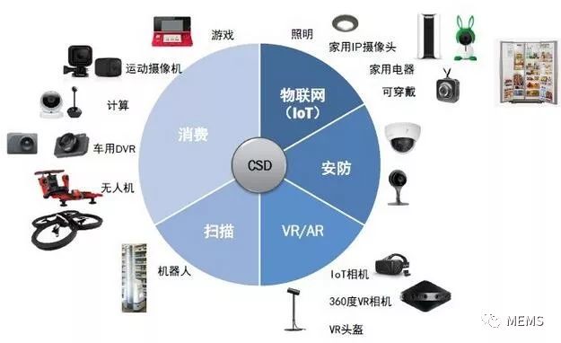
Yi Jihui highlighted China's security video equipment market, which reached 29 billion U.S. dollars in 2016, and showed that 2Mp/1080P will continue to grab VGA and 720P market share. In 2018, 5Mp production will start to grow. trend. At present, the growth drivers of Onsen's image sensors in the consumer sector come from high-end security, scanning, drones, Internet of Things, and OIS/CLAF, with high-end security products growing by 40%. Representative products include: AR0522 product 2 times improvement in near infrared, applied to security; AR0430 won the CES Innovation Award in 2018 with synchronous depth map and red, green and blue (RGB), a single imager synchronization output, a camera can be achieved 3D depth image with extremely low power consumption and up to 120 frames per second.
2 Pin Automotive Connector Housing
2 Pin Automotive Connector Housing,2 Pin Female Male Connector,Auto Wire Harness Connector,Auto Connector And Terminals
Wenzhou Langrun Electric Co.,Ltd , https://www.langrunele.com