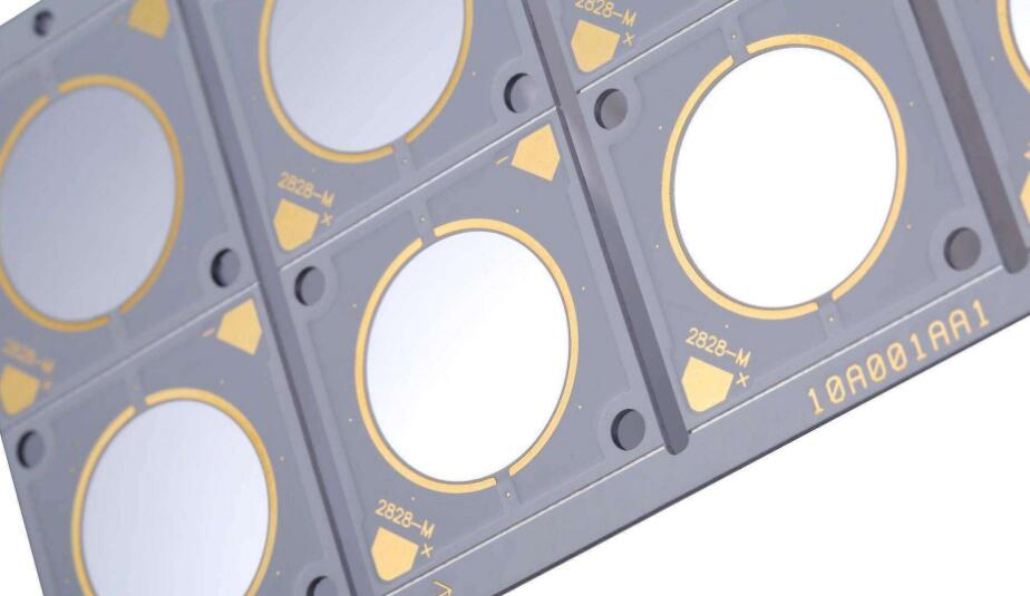
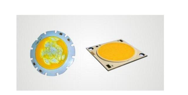
The COB package is called the ChipsonBoard (COB), which is a technology to solve the problem of LED heat dissipation. Compared with in-line and SMD, it features space saving, simplified packaging, and efficient thermal management.
The COB package, that is, the chipOnboard, is to adhere the bare chip to the interconnect substrate with conductive or non-conductive glue, and then perform wire bonding to realize electrical connection. If the bare chip is directly exposed to the air, it is susceptible to contamination or man-made damage, affecting or destroying the function of the chip, so the chip and the bonding wire are encapsulated by glue. This package is also referred to as a soft encapsulation.

1. Ultra-thin: According to the actual needs of customers, PCB board with thickness from 0.4-1.2mm can be used to reduce the weight to 1/3 of the original traditional products, which can significantly reduce the structural, transportation and engineering costs for customers.
2. Anti-collision and compression: The COB product directly encapsulates the LED chip in the concave lamp position of the PCB board, and then is cured by epoxy resin. The surface of the lamp point is convex into a spherical surface, which is smooth and hard, and is resistant to collision and wear.
3. Large viewing angle: The COB package uses shallow well spherical illumination, the viewing angle is greater than 175 degrees, close to 180 degrees, and has a better optical diffuse color dimming effect.
4. Bendable: Bendability is a unique feature of COB packages. PCB bending does not cause damage to packaged LED chips. Therefore, LED arc screens, circular screens, and wavy screens can be easily fabricated using COB modules. . It is an ideal substrate for personalized screens in bars and nightclubs. It can be seamlessly spliced, the production structure is simple, and the price is far lower than the LED shaped screen made by the flexible circuit board and the traditional display module.
5. Strong heat dissipation: COB products are packaged on the PCB board, and the heat of the wick is quickly transmitted through the copper foil on the PCB board. The thickness of the copper foil of the PCB board has strict technical requirements, plus the immersion gold process. Hardly causing severe light attenuation. Therefore, there are very few dead lights, which greatly extend the life.
6, wear-resistant, easy to clean: the surface of the lamp point is convex into a spherical surface, smooth and hard, collision-resistant and wear-resistant; there are dead spots, you can repair point by point; no mask, dust can be cleaned with water or cloth.
7, all-weather excellent characteristics: the use of triple protection treatment, waterproof, moisture, corrosion, dust, static electricity, oxidation, UV effect is outstanding; to meet all-weather working conditions, the temperature difference of minus 30 degrees to zero 80 degrees can still be used normally.

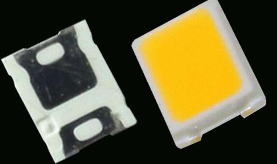
Abbreviation for SurfaceMountedDevices, which means: surface mount device, which is one of the components of SMT (SurfaceMountTechnology). “In the initial stages of electronic circuit board production, via assembly was done entirely by hand. After the first automated machines were introduced, they could place some simple lead components, but complex components still required manual placement for wave soldering. Surface mount components were introduced about twenty years ago and have opened up a new era. From passive components to active components and integrated circuits, they have finally become surface mount devices (SMD) and can be accessed by pick and place equipment. Assembly. For a long time, it was thought that all the lead components could eventually be packaged in SMD.

The assembly density is high, the size of the electronic product is small, and the weight is light. The volume and weight of the chip components are only about 1/10 of that of the conventional plug-in components. After the SMT is generally used, the volume of the electronic product is reduced by 40% to 60%, and the weight is reduced by 60%. 80%.
High reliability and strong anti-vibration ability. The solder joint defect rate is low.
High frequency characteristics are good. Reduced electromagnetic and radio frequency interference.
Easy to automate and increase productivity. Reduce costs by 30% to 50%. Save materials, energy, equipment, manpower, time, etc.
We are a professional screen protector manufacturer, providing one-stop product production solutions, providing exclusive OEM and ODM services. A wide range of products, including HD Clear Screen Protectors, Self-repair Screen Protectors, Anti-microbial Screen Protectors, Matte Screen Protectors, Privacy Screen Protectors and other series.
We are committed to the development, production and sales of hydrogel screen protectors. We strictly control the screen protector production process to ensure that each product meets industry standards. If you want to know more products, please click the product details to view.
Whether you are a group or an individual, we will do our best to provide you with the best service and the most accurate and comprehensive product information!
Universal Screen Protector, TPU Screen Protector, Hydrogel Protective Film, Mobile Phone Screen Protector, Hydrogel Screen Protector, TPU Protective Film
Shenzhen Jianjiantong Technology Co., Ltd. , https://www.tpuscreenprotector.com