We will perform RF line simulation on multi-layer circuit boards. To make a better comparison, the simulation PCB is divided into two boards before surface covering and after grounding; the simulation is compared; the surface is unpatched PCB The file is shown in Figure 1 below (two line widths):
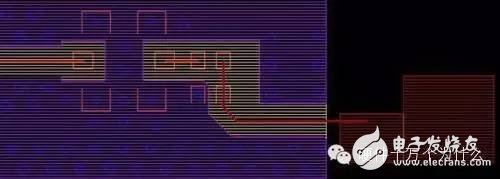
Figure 1a: RF line with 0.1016 mm line width (before surface covering)
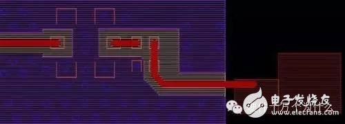
Figure 1b: RF line with 0.35 mm line width (before surface covering)
Figure 1: Surface-not-paved PCB
First, two boards with different line widths (before surface covering) are introduced into SIWAVE from ALLEGRO, and a 50Ω port is added to the target line. For different line widths of 0.1016mm and 0.35mm, our simulation results are shown in Figure 2. The curve shown in the figure is S21, and the simulation frequency range is 800MHz-1GHz.
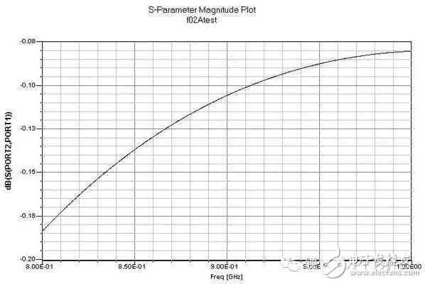
Figure 2a: S21 (line width 0.1016mm) with unsoiled surface
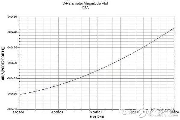
Figure 2b: S21 (line width 0.35mm) with unsoiled surface
Figure 2: S21 with unsurfaced surface
From the figure, we can see that in the range of 800MHz-1GHz, the simulated data is displayed in the order of one to two decimal places. The loss of 0.35mm is an order of magnitude smaller than that of the 0.1016mm line because of the 0.35mm line. The width is close to 50 Ω under the laminate conditions of the plate. Therefore, indirectly verifying that we have done the impedance calculation (with line width constraints) has a certain role.
Next we did the same simulation (800MHz-1GHz) after the surface layer was laid, and the imported PCB file was as shown below.

Figure 3a: 0.1016 mm RF line (surface cover)

Figure 3b: 0.35 mm RF line (surface cover)
Figure 3: PCB after surface coating
The simulation results are as follows:
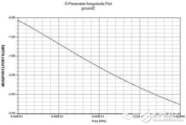
Figure 4a: S21 (0.1016mm) after surface covering
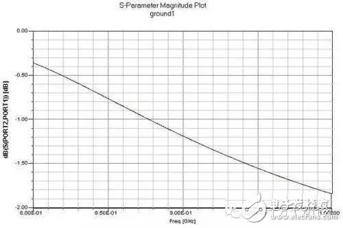
Figure 4b: S21 (0.35mm) after surface covering
Figure 4: S21 after surface covering
It can be seen from the figure that the simulated data shows that the line loss of the transmission line is already on the order of 1-2 dB. Of course, the loss of 0.35 mm is obviously less than 0.1016 mm. Another obvious phenomenon is that compared to the unpatched simulation results, the loss tends to increase as the frequency increases from 800 MHz to 1 GHz.
We can get such a result from the simulation results:
1. It is better to take 50 ohms to walk the RF cable, which can reduce the line loss.
2. The floor covering is in fact coupling part of the RF signal energy to the ground, causing some loss. Therefore, the surface of the PCB should be paved. Try to stay away from the RF line. Engineering experience is greater than 1.5 times the line width.
Fiber Optic Splice Closure,Fiber Optic Splice Case,Fiber Splice Closures,Outdoor Fiber Optic Splice Closure
Cixi Dani Plastic Products Co.,Ltd , https://www.dani-fiber-optic.com