With the continuous development of science and technology and electronics technology, how to easily and effectively realize the problem of uniform display, large-area illumination, high-brightness and high-resolution illumination, and prolong the life of organic light-emitting diodes, etc. It is the technical challenge we face in the future. Today, Xiaobian brings you several examples of active and passive oled display driver designs on weekdays for everyone to use as an electronic design reference.
First, the drive control SSD1303 realizes 96x64 dot matrix PM-OLED
This example uses Solomon's OLED display driver circuit SSD1303, combined with AT89C51 microcontroller to achieve the method of driving OLED display. The SSD1303 is a dedicated OLED display control driver circuit that integrates a controller, row driver and column driver.
In the experiment, the anode material of OLED structure adopts ITO (indium tin oxide), and the cathode uses Mg and other stable metal alloys as Mg:Ag to improve the quantum efficiency and stability of the device, and can form a stable on the organic film. Sturdy metal film.
The PM-OLED uses a common matrix cross screen. The OLED is located between the cross-arranged anode and cathode. By strobing the anode and cathode combinations, the illumination of each OLED can be controlled.
The internal circuit block diagram of the SSD1303 chip is shown in Figure 1:
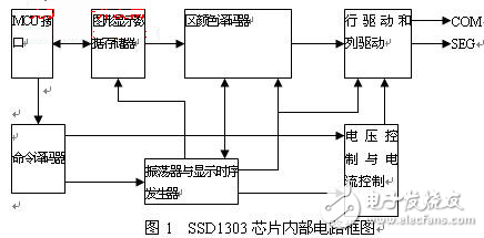
The SSD1303 chip is mainly composed of an MCU interface, a command decoder, an oscillator, a display timing generator, a voltage control and current control, a region color decoder, and a graphic display data memory (GDDRAM), a row driver, and a column driver. This IC's dedicated OLED driver solution optimizes OLED display performance and reduces power consumption. The device is available in a TCP/TAB package. It has a graphic display with a maximum of 132 & TI mes; 64 dot matrix, a logic supply of 2.4 to 3.5V, a power supply of 7.0 to 16V for the OLED panel, a maximum current of 320μA for the column output, and a maximum current of 45mA for the line input. Low current sleep mode less than 5μA, 256 levels of contrast control, programmable frame rate, with several MCU interfaces, such as 68/80 parallel bus and serial peripheral interface, 132 & TI mes; 65bit display buffer, can be scrolled vertically, support Partial display, operating temperature: -40 oC ~ 85 oC.
The whole system consists of three parts: single chip microcomputer, control drive circuit SSD1303 and OLED display. The pins of SSD1303 and MCU interface are: DO~D7 is the data bus interface with the single chip microcomputer, R/W(RW#) is the read/write selection signal. D/C is the data/command selection signal, CS# is the chip select signal, active low, E(RD#) is the enable signal, and RES# is the reset signal. The single-chip microcomputer adopts the low-power and high-performance AT89C51 produced by ATMEL Company. The hardware wiring of AT89C51 and SSD1303 and the display is shown in Figure 2. P1.0, P1.1, P1.2, P1.3 and P1.4 respectively Connected to R/W (RW#), D/C, CS#, E(RD#), and RES# of SSD1303, P0 port is connected to the data bus of SSD1303. Other pins are connected to VCC to 12V, VDD to 2.7V, VSS to ground, and so on. These pins are controlled by the program below so that the OLED displays the desired Chinese characters or graphics. The main program software flow chart is shown in Figure 3.
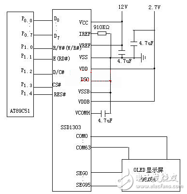
Figure 2 The hardware wiring of the single chip AT89C51 and SSD1303 and the display
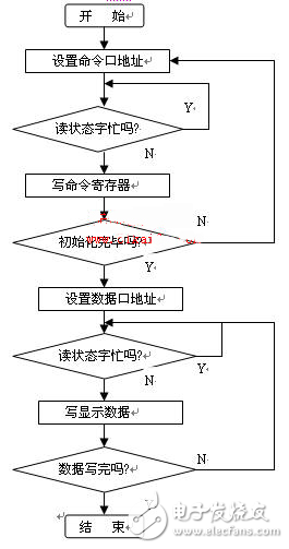
Figure 3 main program software flow chart
Second, Taiwan Pucheng PT6807/PT6808 passive matrix drive mode
This case uses the DC/DC DC boost power supply circuit of ISL97702 portable product, the input voltage is 2.3~5.5V, the output voltage is adjustable in the range of 2~30V according to the load weight; the OLED display driver adopts the passive matrix drive constructed by PT6807 and PT6808. The method is suitable for display driving of monochrome small size OLED.
Just choose ISL97702 as the power IC, you need to consider the device running at the highest efficiency, while reducing power consumption and extending battery operating time. The ISL97702 features a burst mode and dual output voltage selection to maintain converter efficiency and power savings at light load currents. And ISL97702 also has the functions of inrush current limiting, short circuit protection and load isolation during shutdown. ISL97702 DC / DC DC boost power supply circuit diagram, as shown below:
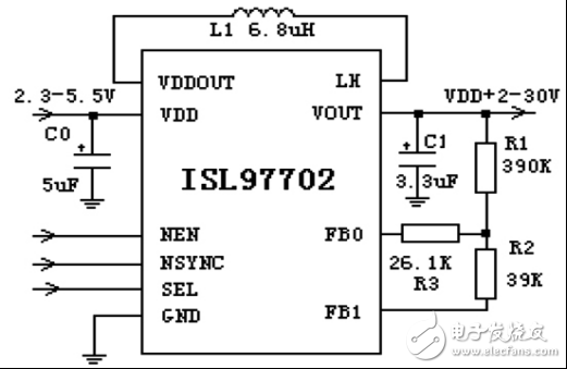
DC/DC DC boost power supply circuit diagram based on ISL97702
The pixels of the OLED display are arranged in a matrix by rows and columns. When displaying images, scanning by row or by column, the basic block diagram of the passive matrix is ​​as follows:
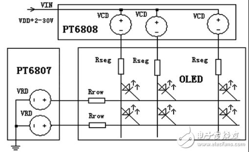
Passive matrix basic structure block diagram
The "row" is sequentially strobed by the common driver PT6807, and the "column" is opened by the column selector PT6808 according to the graphic requirements. For example, if the first row only has the first OLED turned on, it is only about 0.3 mA, and if the second row is that all OLLEDs are strobed, and each row has a total of 100 OLEDs, the total current is about 33 mA. That is to say, the total current is determined by the number of OLEDs in each row, that is, the number of pixels. Since the brightness of an OLED is determined by its current, it is important to keep the current stable. Column drivers typically use a P-channel device as the current source. To ensure that it operates in the saturation region, at least 2 volts is required so that its output current will vary by less than 1% per volt with VDS. When a row has many OLEDs turned on, its total current is relatively large. At this time, there is a large pressure drop at the connection electrode, which lowers the VDS. This pressure drop, in turn, depends on the graphics displayed and is inevitable. Therefore, the sensitivity of the current to be changed by the change of VDS must be minimized. At the same time, the non-uniformity of the output current is also affected by the inconsistency of the driving device. This non-uniformity can be reduced by increasing the VGS operating voltage and the layout matching technique.
128 & TI mes; 128 dot matrix module driver interface, as shown below:
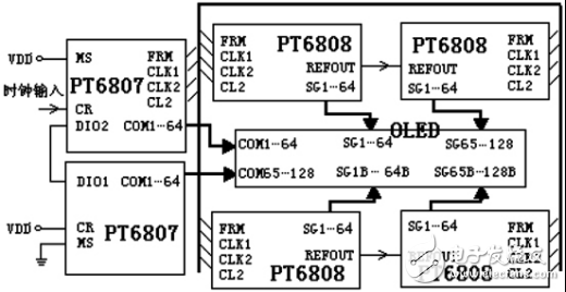
128& TI mes; 128 dot matrix module driver interface diagram
Line drive circuit design
PT6807 is a 64-channel line driver for dot matrix OLED graphic display system. It uses CMOS technology to provide 64 shift registers and 64 output drivers. PT6807 generates its own clock signal to control the PT6808 column driver.
PT6807 can be designed mainly, from two modes, it is convenient for OLED drive display; master/slave mode selection is controlled by control pin MS. In master mode, select MS pin as high level, input/output pin DIO1, DIO2 CL2 is only used as an output pin; in slave mode, the MS pin is set low, the input/output pin CL2 is used as an input, and the state of DIO1, DIO2 is determined by the SHL pin.
Crystal oscillator circuit: In the main mode, the clock frequency can be determined by the R, C, and CR terminals; in the slave mode, the R and C terminals of the crystal oscillator circuit are in a floating state, and the CR terminal is connected to a high level.
Display duty ratio selection: display duty cycle is determined by the state of input pin DS1, DS2; in the main mode, according to DS1, DS2 pin setting to select the duty cycle, there are four duty ratios 1/48, 1/ 64, 1/96, 1/128 are available; in slave mode, DS1, DS2 are connected to power supply VDD.
Shift clock and phase selection: PCLK2 is used to select whether the shift data is shifted on the rising edge or the falling edge of the CL2 clock signal; the selection of the data shift direction is controlled by the MS, SHL pin.
2. Column drive circuit design
PT6808 is a 64-channel column driver for dot matrix OLED graphic display system. It also utilizes CMOS technology and provides display RAM, 64-bit data latch, 64-bit drive and decode logic. The internal display RAM is used to store the data transferred by an 8-bit microprocessor. The display data comes from, which generates a dot matrix OLED drive signal based on the stored data, and is used in conjunction with the PT6807 (row driver).
The input buffer is used to enable and disable the PT6808. When input and output data and instructions are executed, CS1B and CS3 must be in operation. Regardless of the state of CS1B and CS3, both RSTB and ADC can operate normally and the internal state does not change.
The input register is used to interface with the MPU and temporarily store data to be written to the display RAM. When CS1B and CS3 are in operation, the input register is selected by R/W and RS, and the data is written into the input register through the MPU, and then Write to the display RAM, the data is locked on the falling edge of the E signal, and automatically written into the display RAM by internal operations.
Output Register: When CS1B and CS3 are in operation and R/W and RS are high, the output register is used to temporarily store the display data RAM, that is, the stored data in the display data RAM is latched to the output register. When CS1B and CS3 are in operation, R/W is high, and RS is low, status data (busy detection) can be read.
In order to read the contents of the display data RAM, it is necessary to access the read command twice. In the first access, the data in the display data RAM is latched into the output register, and in the second access, the MPU reads the latched data. . That is to say, a dummy read is required when reading the display data RAM, but no dummy read is required when reading the status data.
In order to overcome the problem of automatic off-screen when the brightness of the OLED is high during the working process, the item should be viewed before the data is written, and if the screen is turned off, it is turned on to ensure the normal operation of the OLED screen. Which determines whether the screen is off, if it is closed, it will automatically open the subroutine as follows:
Rs=0; // rs selects the foot for the data/instruction
R_w=1; // r_w is the read/write input pin
e =1; // e is the enable signal input pin
Busy = P3; // P3 is connected to the data line port
e = 0;
If(busy&0x20==0x00) // If true, the screen is off
{com=0x3f; // com is a formal parameter
Wr_command(com);} // wr_command() is a write command subroutine
Third, TFT-OLED analog pixel unit drive / control circuit
The AM-OLED driver implementation includes both analog and digital. In the digital driving scheme, each pixel is connected to a switch, and the TFT is only used as an analog switch, and the gray scale generation method includes a time ratio gray scale and an area ratio gray scale, or a combination of the two. At present, analog pixel circuits still dominate, but in the gray level implementation, the combination of analog technology and time ratio gray scale and area ratio gray theory will be a future development trend. In the analog scheme, the unit pixel circuits can be classified into a voltage control type and a current control type depending on the type of the input data signal.
Voltage controlled pixel circuit
1. Two-tube TFT structure
The voltage control type unit pixel circuit uses a data voltage as a video signal. The simplest voltage-controlled two-tube TFT unit pixel circuit is shown in Figure 1.
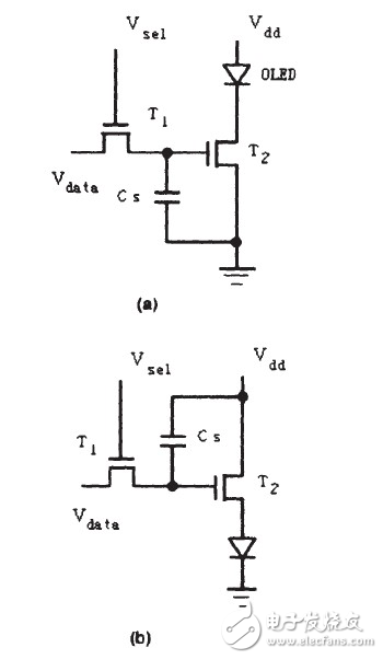
Figure 1 Two-tube TFT driver circuit
The working principle is as follows: when the scan line is selected, the switch tube T1 is turned on, the data voltage charges the storage capacitor CS through the T1 tube, and the voltage of the CS controls the drain current of the drive tube T2; when the scan line is not selected, the T1 is cut off. The charge stored on the CS continues to maintain the gate voltage of T2, and T2 remains in the on state, so the OLED is in constant current control throughout the frame period.
Wherein (a) and (b) are respectively referred to as a constant current source structure and a source follower structure, the former OLED is at the drain end of the driving tube T2, which overcomes the influence of the change of the OLED turn-on voltage on the current of the T2 tube; It's easier to implement. The shortcoming of the two-tube circuit structure is that the inconsistency of the threshold voltage of the driving tube T2 will result in uneven brightness of the display screens, and the current of the OLED and the data voltage have a nonlinear relationship, which is not conducive to the adjustment of the gray scale.
2. Three-tube TFT structure
The voltage control type pixel unit circuit based on the principle of the second generation current transmitter is shown in FIG. 2, the left side of the broken line can be regarded as an external driving circuit, and the right side is a unit pixel circuit.
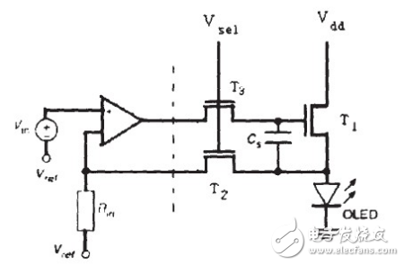
Figure 2 Pixel circuit based on the principle of the second generation current transmitter
In the control mode, T2 and T3 are turned on, and T1 and the operational amplifier constitute the second-generation current transmitter. Since the amplification factor of the operational amplifier can be made large, the threshold voltage of the T1 tube becomes insensitive to the current. Current flowing through T1:
IT1=Vin/Rin
And the source voltage of the T1 tube should be lower than the turn-on voltage of the OLED to prevent the OLED from being turned on. In the hold mode, T2 and T3 are turned off, the storage capacitor Cs maintains the gate voltage of the T1 transistor, and the current enters the OLED via T1. The amplifier is implemented by a COMS circuit, and all of the counterpart pixels can share an operational amplifier.
The simulation results show that although the T3 tube has charge injection and clock feed leakage effect, the OLED current is slightly smaller than the control current. When the nominal current of the OLED is 1μA and the threshold voltage drift exceeds 5V, the relative error of the control current and OLED current is -0.18. %, 5.2%, successfully compensated for the spatial heterogeneity and instability of the TFT.
Although the voltage control type circuit has the characteristics of fast response speed, it is difficult to meet the display requirement because the gray scale of the display cannot be accurately adjusted, and thus a current drive scheme has been proposed. The current control type unit pixel circuit uses a data current as a video signal.
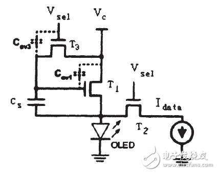
3-tube current control type TFT pixel circuit
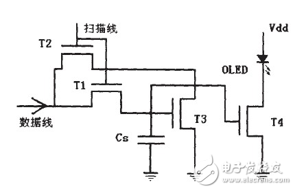
4-TFT current control current mirror pixel circuit
At present, there are already many companies in the world engaged in the research of OLED driver ICs. So far, there is no fully commercialized AM-OLED driver IC. However, NextSierra has introduced separately integrated TFT-OLED row and column driver NXS1008, NXS1009 and control chip NXS1010. Zhang Zhiwei and others use this series of chips to drive 240×320×3 dot matrix TFT-OLED through MCS-51 microcontroller control. The screen realizes a dynamic graphic display with a large amount of information.
Since the supporting driver chip of the liquid crystal display device is relatively complete and inexpensive, the use of such a chip for an active matrix display (AM-OLED) has become a current research focus at home and abroad. The display driver IC is the weak link of the current TFT-OLED. Developing a general-purpose or dedicated driver IC and integrating the control circuit is an important driving force for improving the competitiveness of the OLED in the tablet and display fields.
Digital Timer Switch Sockets,Digital Timer Outlet,Plug-in Time Controller,Plug In Timers,Sockets with Timers
NINGBO COWELL ELECTRONICS & TECHNOLOGY CO., LTD , https://www.cowellsockets.com