Introduction
The high channel density data acquisition system for medical imaging, industrial process control, automated test equipment, and 40G/100G optical communication systems multiplexes the signals of many sensors into at least an ADC, and then sequentially converts each channel. Multiplexing allows fewer ADCs per system, dramatically reducing power consumption, size and cost. Successive approximation ADCs—usually referred to as SAR ADCs based on their successive approximation registers—have low latency characteristics and are therefore suitable for requiring fast response to full-scale input steps (worst case) without any setup A multiplexing system for time problems. The easy-to-use SAR ADC offers low power consumption and small size. This article focuses on key design considerations, performance results, and application challenges associated with multiplexed data acquisition systems using high-performance precision SAR ADCs.
Multiplexed Data Acquisition System Challenge
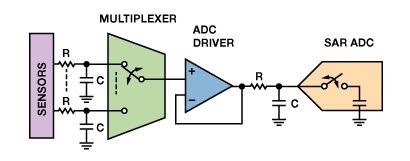
A multiplexed data acquisition system requires a wideband amplifier to quickly establish the full-scale (FS) input range of the ADC. In addition, switching and sequencing the multiplexed channels must be synchronized to the ADC conversion cycle. The large voltage difference between adjacent inputs makes these systems susceptible to crosstalk between channels. In order to avoid errors, the complete signal chain (including multiplexers and amplifiers) must be built to the required accuracy - typically expressed as crosstalk error or setup error. Figure 1 shows a block diagram of a data acquisition system that includes a multiplexer, an ADC driver, and a SAR ADC.

Figure 1. Block diagram of a multiplexed digital acquisition system
Multiplexer
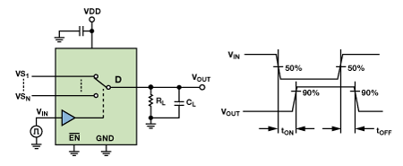
The fast input switching and wide bandwidth performance of the multiplexer are key to achieving high performance. The multiplexer turn-on or turn-off time represents the delay between applying the digital control input and output over 90% of VOUT, as shown in Figure 2.

Figure 2. Switching time for a typical multiplexer
When the multiplexer switches channels, it produces voltage spikes or kickbacks at its inputs. This kickback is a function of turn-on and turn-off time, on-resistance, and load capacitance. Large switches with low on-resistance typically require large output capacitors, and each input switch must be charged to a new voltage. If the output fails to establish a new voltage, a crosstalk error will result. Therefore, the multiplexer bandwidth must be large enough and the multiplexer input must use a buffer amplifier or large capacitor to establish a full-scale step. In addition, the leakage current flowing through the on-resistance will produce a gain error, so both should be as small as possible.
ADC driver
When switching the input channel of a multiplexer, the ADC driver amplifier must establish a large voltage step for the specified sampling period. Inputs can vary from negative full scale to positive full scale, or from positive full scale to negative full scale, so large input voltage steps can be created in a short period of time. The amplifier must have a wide, large signal bandwidth and fast settling time to handle this step. In addition, slew rate or output current limiting can result in non-linear characteristics. At the same time, the driver amplifier must establish a kickback—this kickback is caused by the rebalance of the charge at the input of the SAR ADC at the beginning of the acquisition cycle. This can be a bottleneck in the creation of inputs in a multiplexed system. By reducing the throughput rate of the ADC, setup time issues can be alleviated, providing longer acquisition times, allowing the amplifier sufficient time to build to the required accuracy.
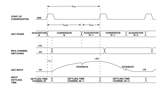
Figure 3 shows a timing diagram of a multiplexed data acquisition system when a full-scale change occurs at the input. The ADC cycle time consists of the conversion time and the acquisition time (tCYC = tCONV + tACQ), which is usually specified as the 1/through rate in the data sheet. At the beginning of the conversion, the DAC ADC's capacitor DAC is disconnected from the input, and the multiplexer channel can switch to the next channel after a short switching delay time tS. This way, you have as much time as possible to establish to the selected channel. To ensure performance at maximum throughput rates, all components in the multiplexed system must complete the ADC input setup between the multiplexer switching and the end of the acquisition time. The multiplexer channel switch must be properly synchronized with the ADC conversion time. The throughput rate achievable by a multiplexed system is equal to the single ADC throughput rate divided by the number of sample channels.

Figure 3. Typical Timing Diagram for a Multiplexed Data Acquisition System
RC filter at the input of the multiplexer
Some designers use a low output impedance buffer to handle kickback from the multiplexer input. The input bandwidth of the SAR ADC (tens of MHz) and the input bandwidth of the ADC driver (tens to hundreds of MHz) are higher than the sampling frequency, and the required input signal bandwidth is usually in the range of tens to hundreds of kHz, so multipath An RC anti-aliasing filter may be required at the multiplexer input to prevent interference signals (aliasing) from folding back into the target bandwidth and alleviating settling time issues. The value of the filter capacitor used for each input channel should be carefully chosen according to the following trade-off conditions: Large capacitors help to attenuate kickback from the multiplexer, but large capacitors also reduce the phase margin of the previous amplifier stage, It is unstable. For high Q, low temperature coefficient, and RC filters with stable electrical characteristics at various voltages, C0G or NP0 type capacitors are recommended. A reasonable series resistance should be chosen to keep the amplifier stable and limit its output current. The value of the resistor should not be too high, otherwise the amplifier will not be able to recharge the capacitor after the multiplexer is backflushed.
Al2O3 Ceramics,Aluminium Oxide Ceramic,Alumina Ceramics,Alumina Ceramic Insulator
Yixing Guangming Special Ceramics Co.,Ltd , https://www.yxgmtc.com