In recent years, the market for printed circuit boards (hereinafter referred to as PCB) has shifted from computers to communications. In the past two years, it has turned to smart phones and tablet-type mobile terminals. Therefore, the HDI board for mobile terminals is the main point of PCB growth. The mobile terminal represented by a smartphone drives the HDI board to be denser and thinner.
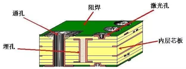
Thin line
PCBs are all developed to high-density thin-line, and HDI boards are particularly prominent. The definition of HDI board a decade ago was that the line width/line spacing was 0.1 mm/0.1 mm and below, and now the industry is basically 60 μm, and the advanced is 40 μm.
PCB circuit pattern formation, the traditional is the photo-imaging chemical etching process (subtraction method) on the copper foil substrate. This practice has many processes, is difficult to control, and has high costs. Current fine line fabrication tends to be semi-additive or modified semi-processed.
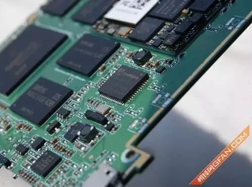
The bonding force between the conductor and the insulating substrate is customary by increasing the surface roughness to increase the surface area and increasing the bonding force, such as strengthening the surface of the roughened resin layer by decontamination treatment, and treating the copper surface with high profile copper foil or oxidation. For thin wires, this physical method guarantees that bonding is not acceptable. Therefore, the electroless copper-plated high-bonding copper foil on the smooth resin surface was developed. If there is a "molecular bonding technique", the surface of the resin substrate is chemically treated to form a functional group which can be closely bonded to the copper layer.
In addition, the dry film imaging pattern transfer during the thin circuit fabrication process, the surface treatment of copper foil is one of the key factors for success. The best combination of surface cleaner and microetcher is used to provide a clean surface with sufficient area to promote dry film adhesion. The surface anti-tarnish treatment layer of the copper foil is removed by chemical cleaning, and the dirt and oxide are removed, and an appropriate chemical cleaner is selected according to the type of the copper foil, followed by micro-etching the surface of the copper foil. In order to make the imaged dry film and the copper layer, the solder resist pattern and the thin line reliable, a method of non-physically roughening the surface should also be adopted.
Semi-additive laminate substrate
Nowadays, the semi-additive method hotspot is to use an insulating dielectric film to laminate, and SAP is more advantageous than MSAP from the realization of fine circuit and manufacturing cost. The SAP laminate uses a thermosetting resin to form via holes and circuit patterns by laser drilling of copper.
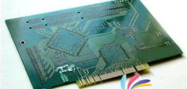
At present, international HDI laminate materials use epoxy resin with different curing agents, adding inorganic powder to improve material rigidity and reduce CTE, and also use fiberglass cloth to enhance rigidity.
Copper plated hole
For reliability reasons, interconnect holes are made of electroplated copper fill holes, including blind via copper and via fill copper.
The ability to fill copper holes is in the form of filling: whether there are voids in the holes closed by copper; flatness: the degree of dimple in the copper-plated opening; thickness-to-diameter ratio: thickness (hole depth) and aperture proportion.
Inverted chip package IC package carrier technology
Organic substrates in global semiconductor packaging account for more than one-third of the market. As the production of mobile phones and tablets increased, FC-CSP and FC-PBGA increased significantly. The package carrier replaces the ceramic substrate with an organic substrate, and the pitch of the package carrier is getting smaller and smaller, and the typical line width/line pitch is now 15 μm.
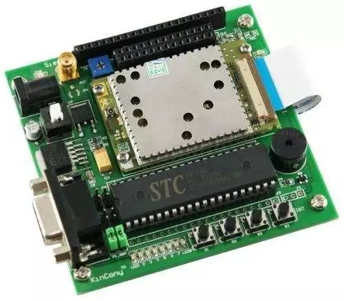
Future development trends. The BGA and CSP fine pitch carrier will continue, while the coreless board and four or more layers of carrier board will be more used. The roadmap shows that the carrier board has smaller feature sizes, and the performance focus requires low dielectric and low. The coefficient of thermal expansion and high heat resistance pursue a low-cost substrate based on meeting performance targets.
Adapt to high-frequency and high-speed requirements
Electronic communication technology ranges from wired to wireless, from low frequency, low speed to high frequency and high speed. Now the performance of mobile phones has entered 4G and will move towards 5G, which means faster transmission speed and larger transmission capacity. The arrival of the global cloud computing era has doubled the data traffic, and the high-speed and high-speed communication equipment is an inevitable trend. PCB is suitable for high-frequency, high-speed transmission. In addition to reducing signal interference and loss in circuit design, maintaining signal integrity, and PCB manufacturing to meet design requirements, it is important to have high-performance substrates.
In order to solve the PCB increase speed and signal integrity, it is mainly for the electrical signal loss attribute. The key factors for substrate selection are dielectric constant (Dk) and dielectric loss (Df). When Dk is lower than 4 and Df is less than 0.010, it is a medium Dk/Df laminate. When Dk is lower than 3.7 and Df is less than 0.005, it is low Dk/. Df grade laminate.
The surface roughness (profile) of the conductor copper in high-speed PCBs is also an important factor affecting signal transmission loss, especially for signals above 10 GHz. Copper foil roughness needs to be less than 1 μm at 10 GHz, and the use of ultra-planar copper foil (surface roughness 0.04 μm) is more effective.
Improve heat dissipation
Along with the miniaturization and high functionality of electronic devices, high heat generation occurs, and the thermal management requirements of electronic devices are increasing. One solution chosen is to develop thermal conductive printed circuit boards. PCBs are required to have high thermal conductivity and heat resistance, and efforts have been made for the past decade. High heat dissipation PCBs such as flat thick copper substrate PCB, aluminum metal based PCB, aluminum metal core double-sided PCB, copper-based planar PCB, aluminum-based cavity PCB, embedded metal block PCB, flexible aluminum-based PCB, etc. .
The metal substrate (IMS) or the metal core printed circuit board is used to dissipate heat from the heat generating component, which reduces the volume and reduces the cost compared with the conventional heat sink and the fan. At present, metal substrates or metal cores are mostly metal aluminum. The advantages of aluminum-based circuit boards are simple and economical, reliable electronic connection, high thermal conductivity and high strength, no lead-free environmental protection, and can be designed and applied from consumer products to automobiles, military products and aerospace.
New trend in flexible and rigid plate technology
The miniaturization and thinning of electronic devices have inevitably used a large number of flexible printed circuit boards (FPCBs) and rigid-flex printed circuit boards (R-FPCBs).
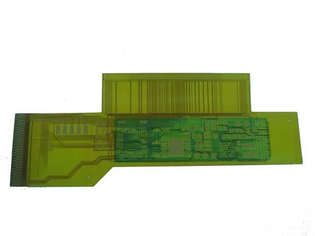
As the application grows, there are many new performance requirements in addition to the increase in number. Polyimide films are colorless, transparent, white, black and yellow, with high heat resistance and low CTE properties, suitable for different occasions. Cost-effective polyester film substrates are also available in the market. New performance challenges include high flexibility, dimensional stability, film surface quality, and film optoelectronic coupling and environmental resistance to meet the changing needs of end users.
FPCB has the same high-speed and high-frequency signal transmission requirements as rigid HDI boards. The dielectric constant and dielectric loss of flexible substrates must be concerned. Polytetrafluoroethylene and advanced polyimide substrates can be used to form flexible circuits. . The addition of an inorganic powder and a carbon fiber filler to the /polyimide resin produces a three-layer structure of a flexible thermally conductive substrate. The inorganic fillers selected are aluminum nitride (AlN), aluminum oxide (Al 2 O 3 ) and hexagonal boron nitride (HBN).
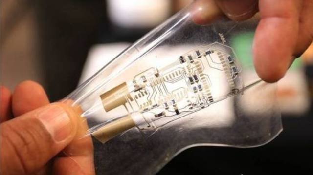
FPCB manufacturing technology, direct metallization on polyimide (PI) film to produce double-sided FPCB technology has been developing, there is a new technology of molecular cement aqueous solution, does not change the surface roughness of PI film can increase and chemical sink Copper layer bonding strength. The chemical bonding of copper is carried out by molecular bonding treatment using a PI film, and a double-sided flexible printed wiring board is produced through a semi-additive process, which simplifies the process and is environmentally friendly, and meets requirements for bonding strength, flexibility, and reliability.
Also using printed autocatalytic electronic circuit technology, in roll-to-roll production (R2R), first printing on the PET film with autocatalytic ink, and then into the electroless copper plating tank, because the ink has autocatalytic ability on the ink A copper layer is deposited to form a copper conductor pattern, and the metal thin line on the PET film is completed.
FPCB application markets such as smart phones, wearable devices, medical devices, robots, etc., put forward new requirements for FPCB performance structure and developed new FPCB products. For ultra-thin flexible multi-layer boards, the four-layer FPCB is thinned from the conventional 0.4 mm to about 0.2 mm; the high-speed transmission flexible board uses low Dk and low Df polyimide substrates to achieve 5 Gbps transmission speed requirements;
High-power flexible board with thick conductor of more than 100 μm to meet the needs of high-power and high-current circuits; high-heat-dissipation metal-based flexible board is R-FPCB for partial use of metal plate substrate; tactile inductive flexible plate, by pressure The sensing film and the electrode are sandwiched between two polyimide films to form a flexible tactile sensor; a flexible flexible plate or a rigid-flexible plate, the flexible substrate is an elastic body, and the shape of the metal wire pattern is improved. adjustable.
Printed electronics
The history of printed electronics is very early, but it has only prospered in recent years. Printed electronics is used in the printed circuit industry as part of printed circuit technology.
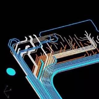
The continuous development of printed electronics shows that the prospects for commercial applications are very broad. Now PCB manufacturers have invested in printed electronics. They started with flexible boards and replaced printed circuit boards (PCBs) with printed electronic circuits (PEC). Printed electronic technology is closest to FPCB. At present, there are many substrates and ink materials. Once performance and cost break through, it will be applied in large quantities, and lowering costs will open up a larger market.
A hybrid system of organic and printed electronics helps the industry grow. The hybrid system of traditional silicon and printed electronic components, which may open up a new PCB industry. These hybrid technologies include large area lithography, screen printing or inkjet printing, and flexible PCB technology.
An important aspect of printed electronics is materials, including substrates and functional inks. In addition to the existing FPCB, flexible substrates also develop higher performance substrates. Currently, there are high dielectric substrate materials composed of a mixture of ceramic and polymer resins, as well as high temperature substrates, low temperature substrates and colorless transparent substrates. , yellow substrate, etc.
In addition to the use of some polymer materials, printed electronics also require functional ink materials, mainly conductive inks, which are constantly improving the conductivity, printing adaptability and low cost. Currently, conductive inks are available for printing electronic products. There are many types. In addition, there are piezoelectric, thermoelectric, and ferroelectric materials that can be used in combination in printed electronics.

Another important aspect of printed electronics is the printing process and the corresponding printing equipment, which is an innovative development of traditional printing technology. Printed electronics can be applied to different printing methods such as gravure, letterpress, screen printing and inkjet printing. Screen printing has been applied in PCB manufacturing, with mature technology and low cost. Currently, it is developing towards automation and high definition.
The range of applications of inkjet printing in PCB manufacturing is expanding, from marking symbols, solder resists to resist patterns, to further direct the printing of conductive patterns; at the same time, inkjet printing is highly refined and rapidly developed. For example, the new aerosol spray technology is significantly superior to piezoelectric spray printing, forming wires with fine and three-dimensional requirements, and can directly print electronic circuits and components on planar or three-dimensional members.
There is also a method of inkjet printing using laser irradiation to instantaneously cure the ink. The thickness and width of the conductive line are 1.0 or more, such as a line width of 10 μm and a line height of 10 μm. For example, a line width of 30 μm and a line thickness of 20 μm are formed on the PI film. FPCB.
The current focus of printed electronics is the low-cost manufacturing of radio frequency identification (RFID) tags that can be printed in rolls. Potential is the field of printed displays, lighting and organic photovoltaics. The wearable technology market is currently a favorable market.
Wearable technology products such as smart clothing and smart sports glasses, activity monitors, sleep sensors, smart watches, enhanced realistic headphones, navigation compass and more. Wearable technology devices are indispensable for flexible electronic circuits, which will drive the development of flexible printed electronic circuits.
Embedded component printed circuit technology
Embedded Component Printed Circuit Board (EDPCB) is a product that enables high-density electronic interconnects. Buried component technology has great potential in PCBs. Embedded component PCB manufacturing technology enhances the functionality and value of PCBs, in addition to applications in communications products, but also provides opportunities in automotive, medical, and industrial applications.
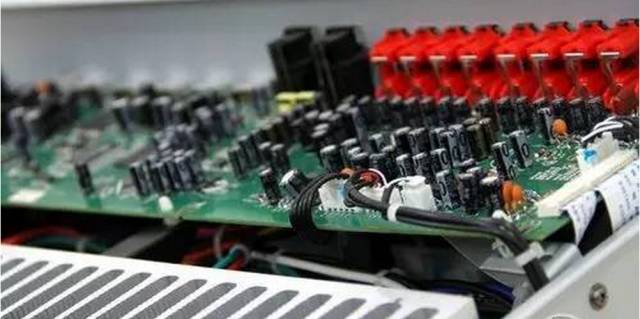
The development of EDPCB, from printed resistors made of carbon paste and thin film resistors made of nickel-phosphorus alloy foil, and planar capacitors with high dielectric constant substrates, to form embedded passive component printed boards, into embedded ICs The chip and the embedded chip component form a buried active and passive component printed board. The problems faced today are the complexity of embedded components and the thinning of EDPCB, as well as heat dissipation and thermal deformation control, and final inspection technology.
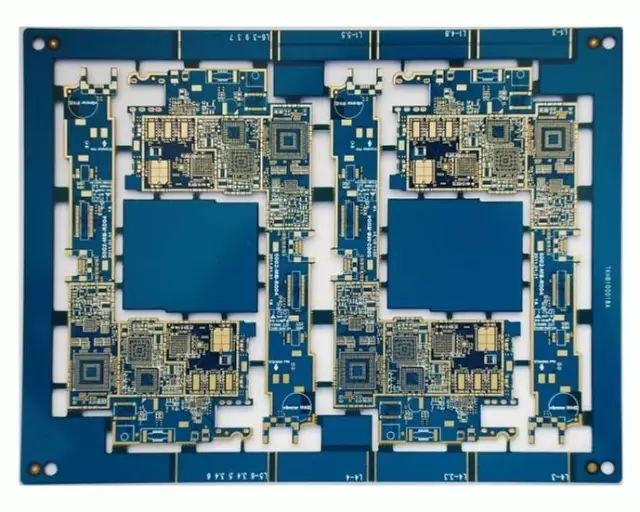
Component embedding technology is now used in portable terminal devices such as mobile phones. The EDPCB manufacturing process enters the practical B2it method, which can achieve high reliability and low cost; there is a PAPAL method, which achieves high-level and low power consumption, and is used in automotive electronics; there is a communication module in which a wafer-level packaged chip is embedded. Reflecting good high-frequency characteristics, eWLB with embedded BGA chips will appear in the future [19]. With the establishment of EDPCB design rules, such products will develop rapidly.
Surface finishing technology
The copper layer on the surface of the PCB needs to be protected in order to prevent oxidation and deterioration of the copper, providing a reliable connection surface during assembly. Some commonly used surface finishes in PCB manufacturing include leaded or lead-free hot air leveling solder, immersion tin, organic solderability protective film, electroless nickel/gold plating, electroplated nickel/gold, and the like.
The surface finish of HDI boards and IC package carriers has evolved from electroless nickel/gold (ENIG) to electroless nickel/palladium/gold (ENEPIG), which helps prevent black discs from appearing after component mounting and affects reliability.
The palladium layer in the ENEPIG coating has been analyzed. The palladium layer structure has pure palladium and palladium phosphorus alloys, which have different hardnesses. Therefore, it is necessary to select different palladium layers for wire bonding and for welding.
After the reliability impact assessment, the presence of trace amounts of palladium increases the thickness of copper-tin growth; while the excessive palladium content produces a brittle palladium-tin alloy, which in turn reduces the strength of the solder joints, thus requiring proper palladium thickness.
From the perspective of the fine line of the PCB, the surface treatment uses electroless palladium/immersion gold (EPIG) to be better than electroless nickel/palladium/immersion gold (ENEPIG), reducing the effect on fine line width/line spacing. EPIG coatings are thinner and do not cause line distortion; EPIG can meet soldering and wire bonding tests.
There are also new direct electroless palladium plating (EP) or direct immersion gold (DIG) on copper, or electroless palladium and autocatalytic gold plating (EPAG) coating on copper, which has the advantage of being suitable for the pressure bonding of gold wire or copper wire. Because there is no nickel layer and there is better high frequency characteristics, the coating is thin and more suitable for fine line patterns, and the process and cost are reduced.
Improvements in the final finish of the PCB, in addition to the introduction of electroless nickel-plated silver (NiAg) coating, silver has good electrical conductivity, solderability, nickel corrosion resistance. The organic coated OSP is improved in properties to improve heat resistance and weldability. There is also an organic-metal composite (OM) coating that has a good price/performance ratio for coating the OM coating on the copper surface of the PCB.
Clean manufacturing
“Green†and “environmentally friendly†are now important signs of PCB manufacturing technology advancement. In addition to trying to adopt revolutionary clean production technologies such as printed electronics and 3D printing, the improvement of existing PCB manufacturing technology to cleaner production is ongoing. Such as the search for materials to replace toxic and hazardous substances, reduce processing steps, and reduce the consumption of chemicals, as well as reduce the amount of water and energy, and the recycling of materials.
Specifically, non-toxic inorganic materials are used as flame retardants, and halogen-free substrates such as electrical, thermal conductivity, and thermal expansion coefficient are also improved; direct laser imaging is used to reduce work processes and material consumption; and semi-additive method is used to reduce electroplating copper and The consumption of etched copper; the use of direct metallization hole process, and the elimination of toxic and harmful substances in the chemical copper bath; the conductive paste printing makes the via hole interconnection process clean and simple.
Direct metallization technology has existed for a long time, and its development has matured over the years. The direct metallization process has carbon black and conductive polymer systems, which are activated by carbon or graphite, conductive polymer instead of palladium, and toxic formaldehyde, cyanide and refractory EDTA complexing agent are eliminated in the chemical copper bath.
The introduction of colloidal graphite direct pore metallization technology has stable dispersibility and good adsorption with a variety of resins. The colloidal graphite direct metallization process has been used in rigid PCB manufacturing for many years. It can now be applied to HDI boards, flexible boards and rigid-flex boards with complex blind holes, buried holes and any layer interconnections, which can reduce process and equipment sites and wastewater. The quantity is beneficial to the environment and improves the production efficiency and the high reliability of the final product [24].
Once known as waste or even hazardous waste in PCB production, it is no longer a “wasteâ€. For example, the excess copper etching solution, the micro etching treatment liquid, and the plating cleaning liquid tend to be recycled online. Some newly designed production line equipment, whether it is etched lines or vertical plating lines and horizontal plating lines, have been considered to be equipped with on-line recycling and regenerative devices, as well as reasonable configuration of air knives in sections, energy saving of circulating pumps, automatic analysis and addition of liquids. Measures such as the life of the liquid medicine are not only conducive to improving the quality, but also conducive to energy conservation and environmental protection.
Printed circuit board manufacturing process
The production of printed circuit boards is very complicated. Here, four layers of printed boards are used as examples to illustrate how PCBs are manufactured.
laminated
Here, a new material called a prepreg is required, which is the core board and the core board (the number of PCB layers > 4), and the adhesive between the core board and the outer layer copper foil, and also acts as an insulation.
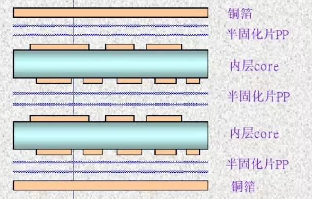
The lower layer of copper foil and the two layers of prepreg have been fixed in advance through the alignment hole and the lower iron plate, and then the prepared core plate is also placed in the alignment hole, and finally two layers of prepreg, a layer of copper foil and A layer of pressure-bearing aluminum plate covers the core.
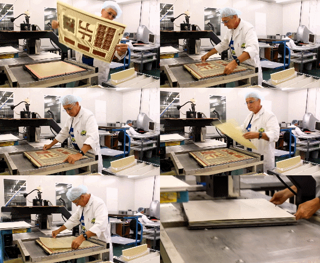
The PCB boards sandwiched by the iron plates are placed on the holders and then fed into a vacuum hot press for lamination. The high temperature in the vacuum hot press melts the epoxy in the prepreg and holds the core and copper foil under pressure.
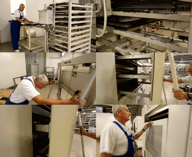
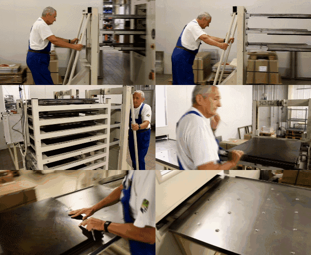
After the lamination is completed, the upper iron plate of the pressed PCB is removed. The pressure-bearing aluminum plate is then removed, and the aluminum plate also serves to isolate the different PCBs and ensure the smoothness of the outer copper foil of the PCB. Both sides of the PCB taken out at this time will be covered by a layer of smooth copper foil.
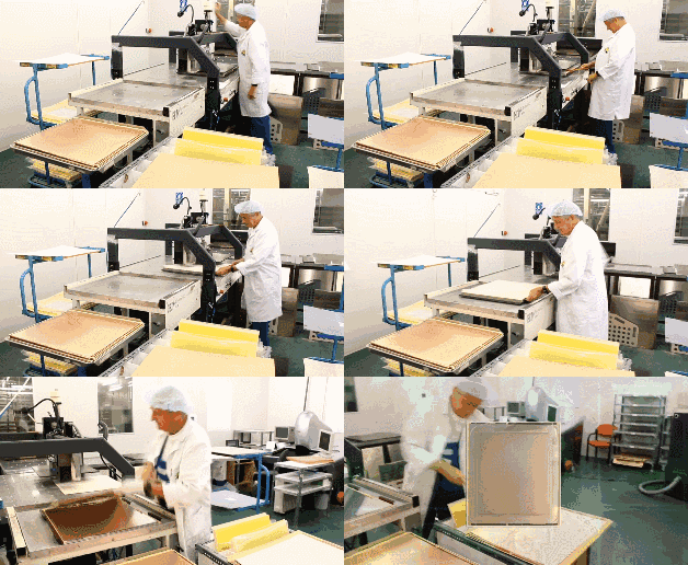
drilling
To connect the four layers of copper foil that are not in contact with each other in the PCB, first drill the perforations through the top and bottom to open the PCB, and then metallize the hole walls to conduct electricity.
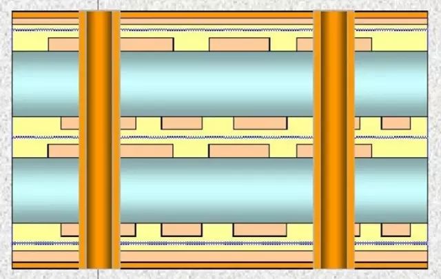
The X-ray drilling machine is used to position the core layer of the inner layer. The machine will automatically find and locate the hole on the core board, and then position the PCB with a positioning hole to ensure that the next hole is drilled from the center of the hole. Over.
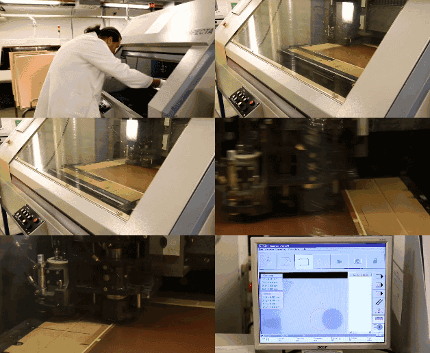
Place a layer of aluminum on the puncher machine and place the PCB on top. In order to improve efficiency, 1 to 3 identical PCB boards are stacked together for perforation according to the number of layers of the PCB. Finally, the uppermost PCB is covered with an aluminum plate. The upper and lower layers of the aluminum plate are used to not tear the copper foil on the PCB when the drill bit is drilled and drilled.

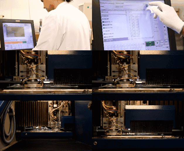
In the previous lamination process, the melted epoxy was extruded outside the PCB, so removal was required. The mold milling machine cuts the periphery of the PCB according to the correct XY coordinates of the PCB.
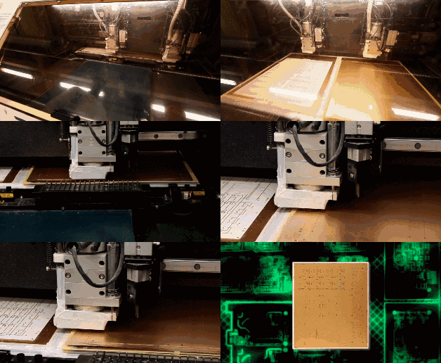
Copper chemical precipitation of pore walls
Since almost all PCB designs are lines of different layers that are connected by perforations, a good connection requires a 25 micron copper film on the walls of the holes. This thickness of copper film needs to be achieved by electroplating, but the walls of the holes are composed of non-conductive epoxy and fiberglass sheets.
So the first step is to first deposit a layer of conductive material on the wall of the hole, and form a 1 micron copper film on the entire surface of the PCB, including the hole wall, by chemical deposition. The entire process, such as chemical processing and cleaning, is controlled by the machine.
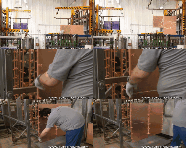
Fixed PCB
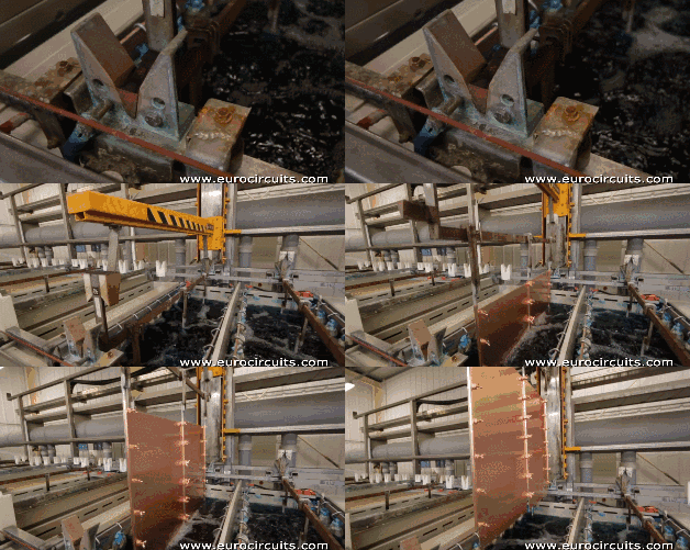
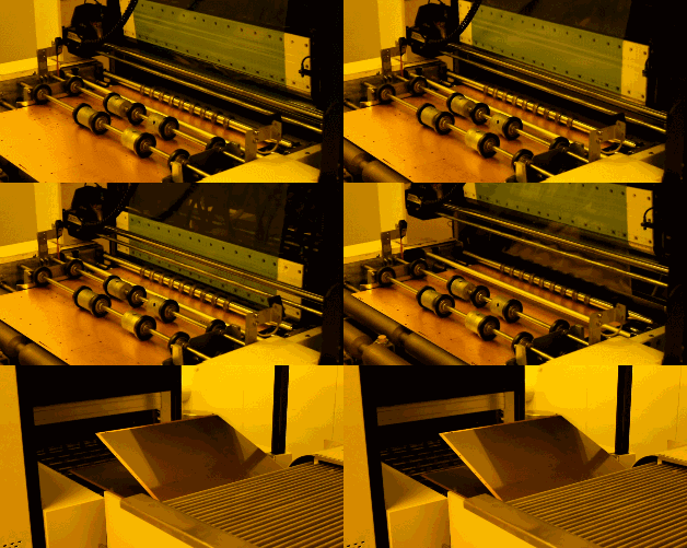
Cleaning the PCB
Shipping PCB
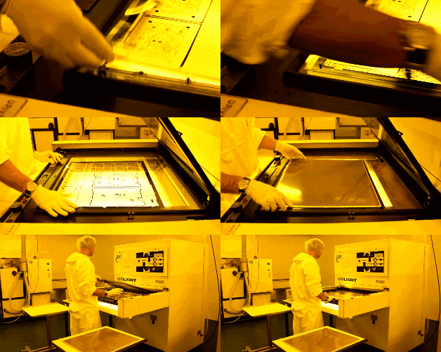
Outer PCB layout transfer
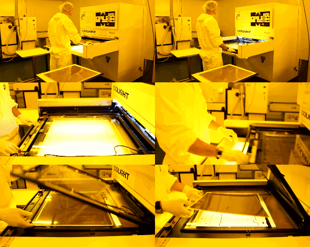
Next, the outer PCB layout will be transferred to the copper foil. The process is similar to the previous inner core PCB layout transfer principle. The photocopying film and photosensitive film are used to transfer the PCB layout to the copper foil, the only difference. It will be a positive film.
The inner layer PCB layout is transferred using a subtractive method, which uses a negative film. The circuit covered by the cured photosensitive film on the PCB is used to clean away the unsolidified photosensitive film, and after the exposed copper foil is etched, the PCB layout line is protected by the cured photosensitive film.
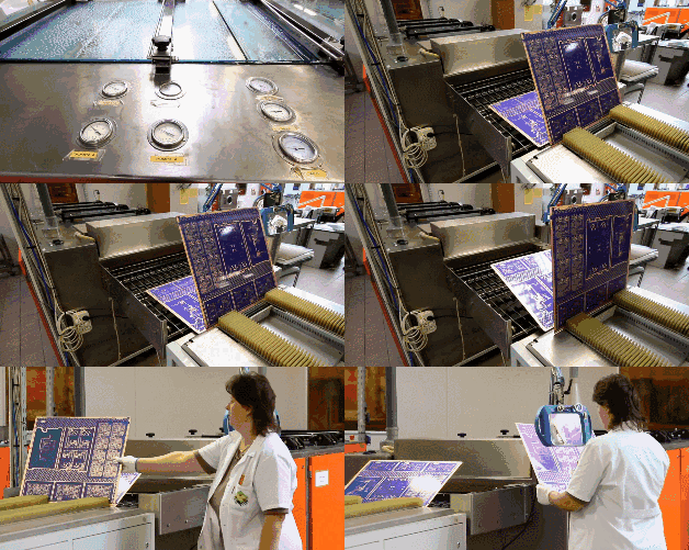
The transfer of the outer PCB layout is based on the normal method, using a positive film. The cured film on the PCB is covered by a non-line area. Electroplating is performed after cleaning the uncured photosensitive film. There is no film at the film, and there is no film, first plated with copper and then tin plated. After the film is removed, alkaline etching is performed, and finally the tin is removed. The line pattern remains on the board because it is protected by tin.
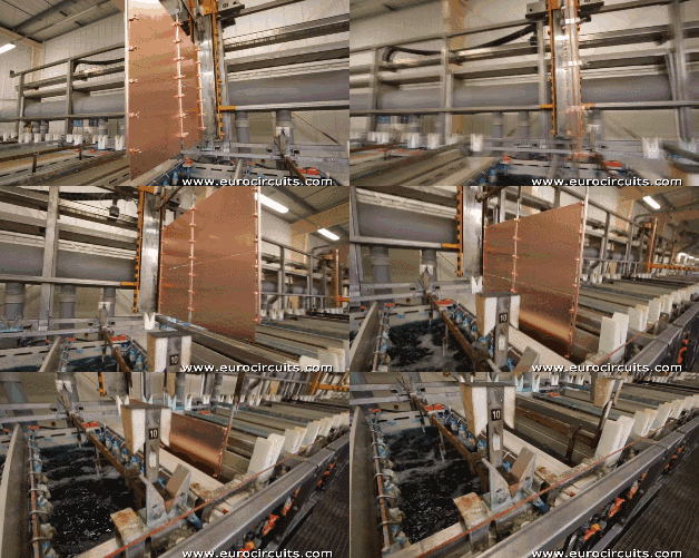
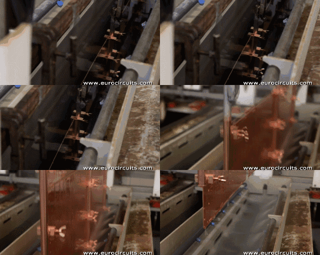
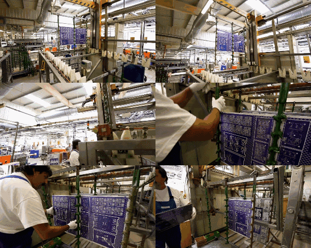
Clamp the PCB with a clip and plate the copper. As mentioned before, in order to ensure that the hole position has sufficient conductivity, the copper film plated on the hole wall must have a thickness of 25 microns, so the whole system will be automatically controlled by the computer to ensure its accuracy.
Outer PCB etching
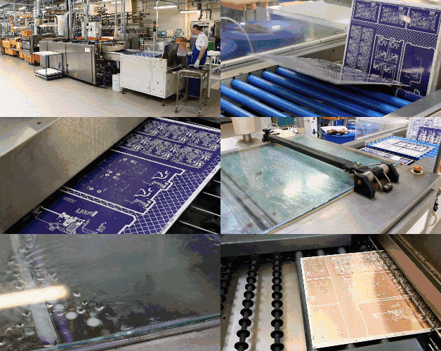
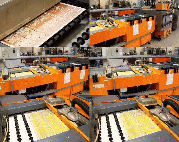
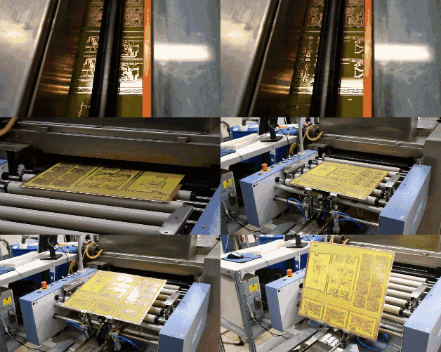
The etching process is then completed by a complete automated pipeline. First, the cured film on the PCB is washed away. The undesired copper foil covered by it is then washed away with a strong alkali. Then remove the tin plating on the copper foil of the PCB layout with tin-removing liquid. After cleaning, the 4-layer PCB layout is complete.
Piezoelectric Buzzer For Driver Circuit Built-in
The piezoelectric buzzers (for Driver Circuit Built-in) offer optimal sound, performance, and efficiency for all types of medical and industrial applications. Our piezo buzzers are constructed in a variety of sizes and work across varying frequencies which allows them to produce different sounds and tones. As voltage is applied to a piezo Buzzer, the piezoceramic disc vibrates, flexing with respect to input voltage to generate sound. Our piezo buzzers maintain low current draw which is advantageous for any battery operated device. Since piezo buzzers don`t have a magnet in their construction, it eliminates EMI/EMC issues.
Buzzer Alarm,Built In Piezoelectric Buzzer,High Frequency Alarm Buzzer,Constant Tone Buzzer For Alarm
Jiangsu Huawha Electronices Co.,Ltd , https://www.hnbuzzer.com