As the complexity of high-speed signal acquisition applications using multiple analog-to-digital converters (ADCs) increases, each converter's complementary clocking solution will determine the dynamic range and potential of the system. As the sampling rate and input bandwidth of the emerging Gigabit Samples per Second (GSPS) ADC increase, the capabilities and performance of the system's distributed sampling clock become critical. System solutions that target high-frequency measurements, such as electrical measurement instrumentation and multi-converter array applications, will require cutting-edge clocking solutions.
Choosing a dedicated auxiliary clock solution is important to prevent the ADC's dynamic range from being limited. Depending on the target input bandwidth and frequency, clock jitter may in turn limit the performance of the ADC. The low jitter and phase noise of the converter's high-speed JESD204B serial interface, the distribution link and alignment capabilities are all clock attributes that are critical to optimizing system performance.
The multi-channel low-jitter GHz clock solution supporting the JESD204B output ADC continues to proliferate in the industry. The design engineer asked us how to choose the right clock solution for its GSPS ADC. Below is the answer and analysis of some of the common discussions related to the technical impact of pairing clock solutions with special ADCs.
The 2nd or 3rd Nyquist frequency region requires low jitter and high speed clocks for high bandwidth input to wideband GSPS ADCs. What effect does clock jitter have on ADC performance?
Since high frequency input signals are used in systems that use GSPS ADCs and direct RF sampling, clock jitter has an increasing impact on system performance. A fixed amount of clock jitter may not limit the performance of a system with low frequency inputs. As the ADC input frequency increases, the same fixed amount of clock jitter can affect the system's signal-to-noise ratio (SNR). The SNR of an ADC is defined as the logarithmic ratio of signal power or noise to the total non-signal power of the input ADC.
When sampling a fast rise time signal at a higher frequency, an ADC sampling instant with a known amount of clock jitter will produce a larger or more blurred sample voltage increment (dV). This is because the slew rate of the high frequency signal is larger than the low frequency signal. Figure 1 shows an example of this relationship:
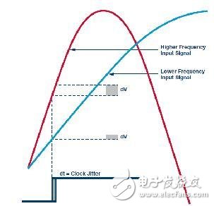
figure 1
After a fixed amount of clock jitter (dt) on the ADC clock, the higher frequency input signal will have a larger sample voltage error, dV, which is associated with the lower frequency input signal. This has a direct impact on the dynamic range capability of the ADC.
What is the difference between peak-to-peak and rms (root mean square) jitter?
There are two types of jitter on the clock signal that directly affect the performance of the ADC: random jitter (RJ) and deterministic jitter (DJ). Deterministic jitter is derived from an identifiable interfering signal whose magnitude is bounded. It is generated by all other unwanted signal characteristics including crosstalk, electromagnetic interference (EMI) radiation, power supply noise, and periodic modulation such as synchronous switching. Deterministic jitter will appear as a spurious signal on the clock signal. These unwanted signals also appear as spurious signals on the digital spectrum produced by the ADC.
The size of random jitter has no bounds and is Gaussian jitter. It can be produced by less predictable effects such as temperature and small semiconductor process variations. If there is enough random jitter on the ADC sample clock, it is possible to increase the noise spectral density (NSD) on the data converter. Add the size of each RJ and DJ rms (RSS) to determine the effect of all jitter on the ADC sample clock.
The random jitter histogram on a typical clock signal should be a perfectly normal Gaussian distribution. Any additional deterministic component of the jitter will produce a bimodal distribution. Peak-to-peak jitter can be measured by making a large number of timing measurements and determining the minimum and maximum jitter deviations. As more measurements progress, the minimum and maximum jitter will eventually continue to expand the absolute peak-to-peak. The effective measurement must be a fixed time and the number of samples measured. Therefore, the absolute peak-to-peak jitter value is not particularly useful unless it is based on a Gaussian distribution with known standard deviation.
The rms jitter is the value of a standard deviation within the Gaussian curve. Even if the sample size is increased, the value will hardly change. This also means that the rms jitter value is more meaningful than the peak-to-peak jitter value and is easier to measure. To make the magnitude of the rms jitter meaningful, the total jitter must be a Gaussian distribution. The deformed Gaussian distribution map indicates the presence of a deterministic jitter component. If possible, the root cause of the deterministic jitter component should be identified and mitigated or eliminated.
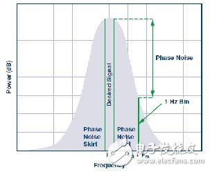
figure 2
Although all power of an ideal clock signal should be within a single frequency point, the actual clock solution will have some "phase noise wave skirt" size. Only a randomly jittered clock signal will form a Gaussian distribution. Any deterministic jitter will distort the ideal Gaussian profile. The phase noise power at any point on the curve can be measured from the peak at F0 to the target frequency at F0 + Fm.
How does the input clock jitter of the ADC reduce the performance of the SNR and NSD?
The NSD of the ADC is one of the main performance indicators of the converter. NSD defines the overall noise power per unit bandwidth (sampled at the corresponding ADC sampling frequency (fS)). NSD is a function of the ADC's full-scale signal-to-noise ratio (SNRFS) and arbitrary clock jitter reduction and noise distribution over the spectrum's Nyquist bandwidth (fS/2). Any sampling time error will cause some parts of the noise signal power to drop.
As clock jitter increases, some portion of the target sampled signal power will be spread out of its discrete frequency point with a Fast Fourier Transform (FFT) and then become part of the noise power. This is because the sampling time of the signal near the phase noise of the clock signal is not ideal. Figure 2 shows a visual example of how the phase noise "wave skirt" bleeds power from an ideal target signal in the frequency domain.
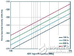
image 3
The ideal NSD performance of an ADC operating at 1 GSPS is limited by the rms coded clock jitter. The rms jitter of the clock may limit the dynamic range of the ADC at higher input frequencies.
To get the total SNR drop of the ADC, the square root of the sum of the jitter noise power and the standard SNR of the ADC at the target signal frequency should be calculated. When the ADC sample clock jitter is low enough, SNRadc = SNR drops because the converter's internal aperture jitter and nonlinearity will limit its SNR. Conversely, a sampling clock with increasing jitter will eventually become a limiting factor in ADC SNR performance. This will become more and more obvious because the frequency of the target signal is higher. The output noise of all achievable ADCs is limited by SNR performance. As the input level increases or decreases, the jitter noise component will change accordingly.
The NSD of the ADC can be calculated by subtracting the SNR drop of the full-scale input power of the ADC from the noise power, which is a function of the Nyquist frequency. This value can be obtained by the following formula.
NSDADC = PowerADC_FS – SNR drop (dBFS) – 10log(fS/2)
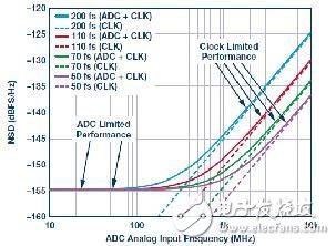
Figure 4
This figure shows a 14-bit wideband converter that is internally quantized and linearly limited to –155 dBFS/Hz NSD at low analog input frequencies (<100 MHz), regardless of whether the external rms clock jitter reaches 200 Fs. In this case, the system clock jitter will determine the NSD performance at high analog input frequencies (>100 MHz) based on its rms amplitude.
For example, Figure 4 shows the NSD impact of a 14-bit 1 GSPS ADC with wide input bandwidth and multiple clock jitters. When sampling a signal from 10 MHz to 100 MHz, even a very high clock jitter of 200 fs does not significantly impair the NSD performance of the ADC (–155 dBFS/Hz). However, when sampling an input signal at 1 GHz or 2 GHz, the 200 fs rms jitter of the clock will significantly limit ADC performance compared to low rms clock jitter. When sampling a 2 GHz signal, a 200 fs rms jitter will result in an 12 dB increase in ADC noise associated with the target signal power (compared to a 50 fs rms clock jitter).
Part of the GSPS ADC allows the fast input clock multiple to be split internally within the ADC to derive the actual sample clock. What are the advantages and disadvantages of using a higher rate sampling clock for the ADC in this case?
Unlike an option that allows only one option to input the clock frequency at 1&TImes; the actual sample rate, some ADCs allow the use of higher rate clock rates, such as 2&TImes;, 4&TImes; or 8&TImes; sampling rate. The ADC can then be configured to internally divide the higher frequency clock into a lower clock rate that samples the analog signal to the ADC. This type of configuration has several advantages.
The first advantage is that the system board can now handle multiple sample rates using the same hardware and clocking solution. In this case, using a faster or slower sampling rate requires only a slight change to the ADC's software registers. For example, using the ADC's electrical test and measurement solutions at the highest clock rates, such as digital sampling oscilloscopes, now you can provide end users with multiple sample rate options by simply touching the GUI button. In this way, you can also market segment the same board with only software version differences. The two ADCs that provide this feature are the AD9680 and AD9234, which are 1 GSPS converters with 14-bit and 12-bit resolution, respectively.
The second advantage is that ADCs with higher clock frequencies have higher performance than using a lower 1× sampling rate. Higher frequency clocks provide faster signal slew rates and therefore have more accurate edges and lower jitter. As mentioned earlier, assuming that ADC jitter is not a limiting factor, the lower jitter clock itself can achieve lower NSD and higher SNR.
A third advantage is the elimination of an additional clock frequency for the timing device and the board traces. This allows the system to operate with a smaller clock signal multiple and reduces overall timing complexity. The RF clock signal may be used as an input to a portion of the ADC that allows the slower sampling clock to use the internal split function.
One potential challenge with this sampling configuration is the need to determine the actual timing device that can achieve low jitter at increased frequency multiples. This challenge has been somewhat mitigated as clock solutions with higher frequencies, performance, and channel counts have been released and applied to system boards. However, the endless demand for higher sample rate converters and complex companion clock devices has not diminished.
How do I get the frequency domain phase noise curve from the clock device and determine the time domain rms jitter for the specific ADC sample clock frequency?
Although the two describe the same phenomenon, it may be counterintuitive to associate the phase noise of the clock with a particular jitter value. Although the two are related, engineers need to cross the frequency and time domain to match. The phase noise curve is plotted in the frequency domain and the root mean square jitter component of the clock signal is reflected as a time domain value.
Multiplication in the time domain is similar to convolution in the frequency domain. Any phase noise ripple or phase modulation spurious noise on the clock is convolved into a digital signal for the ADC. The level or magnitude of the noise convolution on the clock coupled to the sampled output is as shown in the following equation.

Sampling output
clock
The frequency domain in Figure 5 shows an example of a phase noise curve for the clock signal. The X-axis shows the frequency offset relative to the carrier, in this case the 983 MHz clock. The Y-axis is the phase noise density expressed in dBc/Hz (dB ​​power associated with the carrier power in Hertz). It should be clear from this curve that when phase noise is further observed at the frequency on the clock, the associated noise floor is created and the amplitude of the gradually increasing cumulative phase noise is reduced.
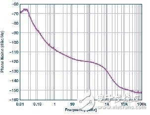
Figure 5
This curve shows the phase noise that crosses the frequency offset on the carrier clock at 983 MHz in dBc/Hz. This information can be used to derive clock jitter.
The rms jitter of the clock signal can be calculated from the phase noise curve by integrating the area under the curve in segments of ten octaves. Although there are now online calculation tools that can calculate jitter from phase noise, this can be done using several mathematical formulas.
It is not practical to try to calculate accurate jitter by adding each 1 Hz offset point. Therefore, a very close rms jitter can be obtained by obtaining the phase noise slope of each decade octave with the dB/decade value between the endpoints. Ideally, the wideband phase noise will be combined into a larger offset equal to the sampling frequency. However, to ensure that the instance calculations are bounded, we can calculate the rms jitter in a typical wired application. Let's take a look at the phase noise curve in Figure 6, which calculates the jitter in the 10 kHz to 20 MHz offset of the 983 MHz carrier.
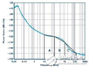
Figure 6
The phase noise ten octave segmentation curve derived from Figure 5 can be subdivided into three segments to calculate the rms jitter between the 10 kHz to 20 MHz offset of the 983 MHz frequency carrier.
The total rms jitter is the sum of the areas below the curve between the two target frequencies. In this case, the estimated area is displayed in three segments labeled A, B, and C. The slope of the phase noise curve between each segment endpoint can be easily estimated and will then be used for calculations. The relationship between the period jitter JPER over the entire phase noise spectrum L(f) is as follows:
![]()
The RMS JPER in a particular frequency band between (f2 – f1) can be calculated from:

When the frequency axis of L(f) is a logarithmic scale, the piecewise function can be used to estimate the phase noise. Therefore, L(f) can be rewritten as:
![]()
Where K-1 is the number of segments in the piecewise function, b is the phase noise magnitude of the start frequency of the octave, a is the estimated slope in dB/decade, and U(f) is the step function .
If we substitute L(f) in Equation 3 into Equation 2, we can get:
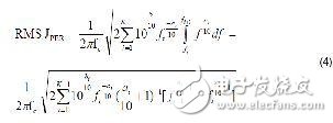
The root mean square jitter can then be calculated using the values ​​of each segment of the graph of Figure 6, where fc = 983 MHz:
A: a = –3.44 dB/decade, starting frequency f = 10 kHz, b = –116.91 dBc/Hz
B: a = –9.75 dB/decade, starting frequency f = 100 kHz, b = –120.35 dBc/Hz
C: a = –18.58 dB/decade, starting frequency f = 1 MHz, b = –130.1 dBc/Hz
RMS JPER = 151 fs
The latest GSPS ADC uses the JESD204B serial output instead of the multiplexer bank for the LVDS output. How can a clock solution use JESD204B to align multiple ADCs in a system to a single sample?
The multi-channel low-jitter GHZ clocking solution pairs the system reference timing signal with the corresponding clock output defined in the JESD204B specification with a signal called SYSREF. The SYSREF signal is the absolute timing reference signal for the JESD204B link used within the system. Multiple instruments, sensor arrays, and radar systems all need to align the timing of multiple simultaneous ADCs (2, 4, 8, 16 ... 100s) into as few sample ranges as possible. For such applications, the timing flexibility of the clocking solution is important to de-skew and align the SYSREF signal to each corresponding ADC clock.
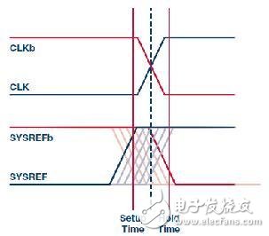
Figure 7
Multiple clock output pairs may be skewed in phases associated with each other and their associated auxiliary SYSREF signals. Coarse and fine-tuned timing allows the clock and SYSREF to be synchronized across a range of ADCs.
A system with 16 ADCs may require four separate acquisition boards, each with four ADCs and directly connected together via an electrical backplane. Each ADC can see the associated sample clock edge instant at different times based on its spatial location relative to each other and the intersection between the traces.
In some cases, the clock and associated SYSREF need to be aligned to the same point in time for each ADC. In other systems, the clock phase needs to be deliberately misaligned to account for the phase difference of the input signal between a series of ADCs. For the intersection of two or four ADCs, the clock may need to be reversed or phase adjusted for a specific 90° increment. In any case, the JESD204B clocking solution provides independent skew between each ADC clock and SYSREF pair to function as an acquisition system.
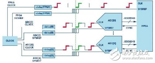
Figure 8
For the JESD204B ADC and DAC, the new clock chip solution is able to align multiple outputs to a single or periodic SYSREF signal. This feature eliminates the propagation time difference caused by the spatial clock routing delay between the ADC acquisition time and the clock source.
What clock solutions does the GSPS ADC offer?
The phase noise or time domain jitter of a GHz clocking solution is a primary performance factor to consider when selecting a clock source for a GSPS ADC. For acquisition systems that require a large number of ADCs, the best clocking solution also requires a large number of output channels to achieve their respective encoding rates. A secondary performance factor is the ability to synchronize the system's reference parameters within the JESD204B link, which further enhances the clock system's capabilities.
The AD9525 provides a 3.3 GHz output clock pairing with only seven rms jitter of only 50 fs and can be used as a SYSREF dedicated synchronous output within the frame of the JESD204B interface.
The AD9528 provides not only seven 1 GHz output clock pairs, but also an auxiliary SYSREF signal, each of which can be skewed to align the corresponding ADC within a single sample alignment pulse.
The HMC7044 is a high performance 3 GHz 14 output jitter attenuator with JESD204B SYSREF support.
in conclusion
The amplitude of the encoded clock phase noise and jitter of the latest high bandwidth and wideband ADCs needs to be gradually reduced. Although many clocking solutions can be used with these high frequency ADCs, solutions with very low phase noise and the ability to synchronize many ADCs are the best solution.
The phase noise curve of a typical clocking solution can be converted to the time domain to determine the rms jitter and the potential impact on the dynamic range of the ADC. Another advantage of advanced clocking solutions is the unique SYSREF that can skew the clock signal pairing within the JESD204B frame. The critical auxiliary clock components selected for the GSPS ADC may maintain or degrade the performance of the ADC, depending on the frequency of the target acquisition signal.
security service,outdoor camera security,home cameras,home security camera system
Dongguan Metalwork Technology Co., LTD. , https://www.diecast-pro.com