PCBA process
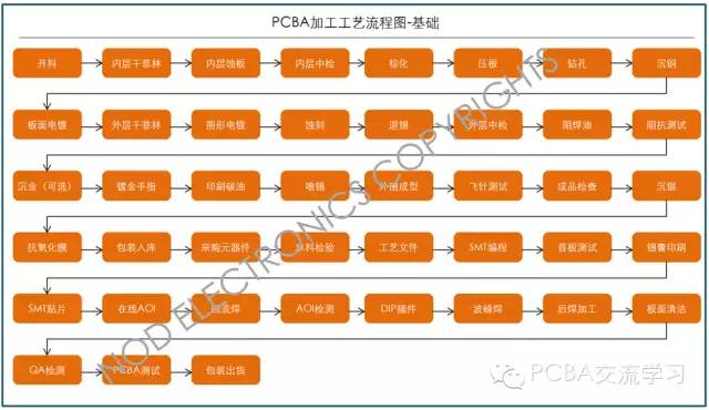
PCBA process is very complex, basically going through nearly 50 procedures, from the circuit board process, component procurement and inspection, SMT chip assembly, DIP plug-in, PCBA testing, program firing, packaging and other important processes. Among them, the circuit board process has 20 to 30 processes, and the procedure is extremely complicated. The PCBA processing flow is shown in detail in the following figure, allowing you to quickly acquire relevant expertise.
PCBA process flow chart
Circuit board equipment includes electroplating wire, sinker wire, DES wire, SES wire, washer, OSP wire, sink nickel wire, press, exposure machine, oven, AOI, screeding machine, edger, and cutting Machines, vacuum packaging machines, boring machines, drilling rigs, air compressors, spray guns, CMI series, light drawing machines, etc.
The circuit board can be divided into single-sided, double-sided, and multi-layer printed boards according to the number of conductor patterns. Single-sided basic manufacturing process is as follows
Foil--> blanking--> baking sheet (preventing deformation)--> molding--> washing, drying--> foil (or screen printing)->exposure development (or anti-corrosion ink)- -> Etching -> Defilming -> Electrical continuity test -> Cleaning process -> Screen printing solder mask pattern (oil) -> Curing -> Screen printing mark symbol -> Curing - -> Drilling -> Forming -> Cleaning and Drying -> Inspection -> Packaging -> Finished Product.
The basic manufacturing process for a double panel is as follows:
Graphic plating process
Foil--> blanking-> Drilling reference hole--> CNC drilling--> Inspection--> Deburring--> Electroless plating of thin copper--> Electroplated thin copper--> Inspection--> Brush plate -> Foil (or screen printing) -> Exposure development (or curing) -> Inspection repair plate ----> Pattern plating (Cn ten Sn/Pb) -> Defilming -> Etching - -> Inspection plate-->Plug nickel-plated plating-->Hot-melt cleaning-->Electrical continuity inspection-->Cleaning process-->Screen printing resist pattern-->Curing-->Screen printing symbol- -> Curing -> Shape Processing -> Wash Dry -> Inspection -> Packaging -> Finished Products.
The main advantage of the SMOBC process is that it solves the problem of solder bridging and short-circuiting between the thin lines. At the same time, due to the constant lead-tin ratio, it has better solderability and storage than the hot melt plate. The SMOBC process of retreating lead-tin from the pattern plating process is similar to the pattern plating process. Only changes after etching. Double-sided copper clad plate--> According to the pattern electroplating process to the etching process-->Lead lead-->Check---->Cleaning--->Welding resist pattern-->Plug nickel plating gold--> Plug-adhesive tape-->Hot air leveling---->Cleaning--->Screen printing mark symbol--->Outline processing--->Cleaning and drying--->Product inspection-->Packaging-->finished product.
SMT processing technology1. According to the customer Gerber file and bill of materials, production SMT production process files, generate SMT coordinates file
2. Check whether all the production materials are available, make a uniform slip, and confirm the PMC plan for production.
3. SMT programming, and make the first board to check to ensure that there is no mistake
4. According to SMT process, making laser steel mesh
5. Solder paste printing to ensure uniform paste after printing, good thickness and consistency
6. Mount the components on the circuit board through the SMT placement machine, and perform on-line AOI automatic optical inspection when necessary
7. Set a perfect reflow oven temperature curve, let the circuit board flow through the reflow solder paste, paste from the paste, liquid to solid state conversion, cooling can be achieved after a good welding
8. After the necessary IPQC inspection
9. DIP plug-in process inserts plug-in material through the circuit board and then flows through wave soldering for soldering
10. The necessary after-baking processes, such as cutting feet, post-welding, board cleaning, etc.
11.QA conducts a full inspection to ensure the quality is OK

PCBA tests the most critical quality control process in the entire PCBA manufacturing process. It strictly follows the PCBA test standard and tests the test points of the circuit board according to the customer's test plan.
The PCBA test also includes five main forms: ICT testing, FCT testing, aging testing, fatigue testing, testing in harsh environments. Among them, the ICT (In Circuit Test) test mainly includes circuit on/off, voltage and current values ​​and fluctuation curves, amplitudes, noise, etc.; and FCT (Functional Circuit Test) testing requires IC program firing, and the function of the entire PCBA board. Conducting simulation tests to find problems in hardware and software, and equipped with necessary production fixtures and test racks; Burn In Test is mainly to electrify PCBA boards and electronic products for a long time to keep them working and observe whether they appear. In case of any failures, the electronic products after aging test can be sold in batches; the fatigue test is mainly sampling the PCBA board, and performing high-frequency, long-time operation of the function to observe whether there is failure, such as continuous clicking of the mouse up to 100,000 times. Or switch off the LED lamp 10,000 times and test the probability of failure to feedback the working performance of the PCBA board in the electronic product; the test in the severe environment (Severe Conditions) mainly exposes the PCBA board to the limit value of temperature, humidity, Drops, splashes, and vibrations were obtained, and random sample test results were obtained to infer the reliability of the entire PCBA board batch product.
Eyeglass frames are an important part of eyewear, mainly supporting the lenses and providing an aesthetic effect. The materials used are mainly metal, plastic or resin, natural materials and so on. A fine eyeglass frame should be made of a stable, safe, reliable and skin-friendly material that is light, strong and does not deform.
We custom etching eyeglass frames with drawings provided by customers. The raw material we more use for spectacle frame is stainless steel. The thickness we can achieve is 0.03-1.0mm. We are equipped with professional metal etching equipment and exposure development equipment. Our customized metal eyeglass frames can achieve burr-free finishes, no notch.
Etching Eyeglass Frames,Spectacle Frame,Customized Metal Eyeglass Frames,Chemical Etching Eyeglass Frames
SHAOXING HUALI ELECTRONICS CO., LTD. , https://www.cnsxhuali.com