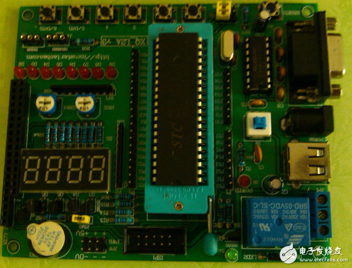
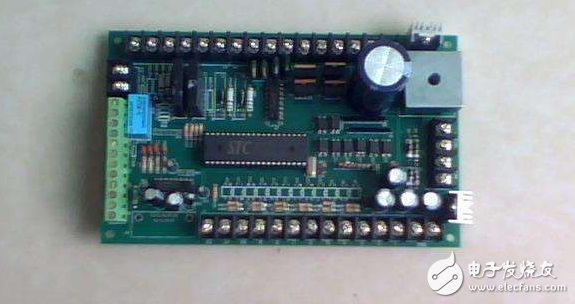
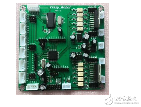
The process of executing a program by a microcontroller is actually the process of executing the program we have programmed. That is, the process of instruction by instruction. Each step of the computer can be divided into three phases. That is, the instruction-----analysis instruction-----execution instruction.
The task of fetching instructions is to read the current instruction from the program memory according to the value in the program counter PC and send it to the instruction register.
The task of analyzing the instruction phase is to take out the instruction opcode in the instruction register, decode it, and analyze the nature of the instruction. If the instruction requires an operand, look for the operand address.
The process of the computer executing the program is actually repeating the above operation process one by one, until the stop instruction can be cycled to wait for the instruction.When a general computer is working, the program and data are first sent to the memory through the input interface circuit and the data bus through an external device, and then taken out one by one. However, the programs in the microcontroller are generally fixed in the on-chip or off-chip program memory by the writer in advance. Therefore, the instruction can be executed upon startup.
Below we will give an example to illustrate the execution of the instruction:

At startup, the program calculator PC becomes 0000H. Then the microcontroller automatically enters the execution program process under the action of the sequential circuit. The execution process is actually a loop process of fetching instructions (taking out the stage of instructions stored in memory beforehand) and executing instructions (analysing and executing instructions).
For example, the execution instruction: MOV A, #0E0H, its machine code is "74H E0H", the function of this instruction is to send the operand E0H to the accumulator, 74H has been stored in the 0000H unit, and E0H has been stored in the 0001H unit. When the microcontroller starts running, it first enters the fetching phase, in the order:
1 The contents of the program counter (in this case, 0000H) are sent to the address register; 2 The contents of the program counter are automatically incremented by 1 (becomes 0001H); 3 The contents of the address register (0000H) are sent to the memory through the internal address bus to the address in the memory. Decode the power to make the unit with the address 0000H selected; 4 The CPU makes the read control line valid; 5 The content of the selected memory unit (which should be 74H) under the control of the read command is sent to the internal data bus because it is taken Refers to the phase, so the content is sent to the instruction register via the data bus.At this point, the instruction phase is completed and enters the stage of decoding analysis and execution instructions.
Since the content entered into the instruction register is 74H (opcode), after decoding by the decoder, the microcontroller knows that the instruction is to send a number to the A accumulator, and the number is the next one in the code. Storage unit. Therefore, to execute the instruction, the data (E0H) must be taken out of the memory and sent to the CPU, that is, the second byte is also taken in the memory. The process is very similar to the fetching phase, except that the PC is already 0001H. The instruction decoder, in conjunction with the timing component, generates a micro-operation series of 74H opcodes that cause the digital E0H to be fetched from the 0001H unit.

Because the instruction is required to send the fetched number to the A accumulator, the fetched number enters the A accumulator via the internal data bus instead of entering the instruction register. At this point, the execution of an instruction is completed. PC=0002H in the single-chip microcomputer, the PC automatically adds 1 every time the CPU fetches or retrieves the memory, and the MCU enters the next fetching stage. This process is repeated until a pause command is received or the loop waits for a command pause. The CPU executes the instructions one by one to complete all the specified functions.
For a mcu, the performance description will tell sram, the size of the flash size, for beginners, will not consider and pay attention to these things, get things only use. In fact, these quantities are very important. Think about it, why the code can run, the amount of code, and how the variables of the defined int, short, etc. are allocated and stored. relationship.First of all, the memory of the MCU can be divided into ram and rom. The difference between ram and rom is no longer explained here. We can equivalent it to flash and sram, which can be obtained according to the definition of flash and sram. Can be saved, sram can not, but sram execution speed is faster than flash, you can divide the microcontroller program into code (code storage area), RO-data (read-only data storage area), RW-data ( Read and write data storage area) and ZI-data (zero initialization data area). The value of these 4 quantities in the code can be observed under the MDK compiler, as shown in Figure 1 below:
figure 1:

The code and RO-data are stored in the flash, so the sum of the two is the size of the space that the flash needs to allocate to the microcontroller (and equal to the size of the .bin file generated by the code), and the RW-data and ZI-data are stored in In sram, the sum of the two is the size of the space that the sram needs to allocate to them in the microcontroller.
In addition, we must think of the stack, stack, global (staTI), literal constant area and program code area and the relationship between code, RO-data and so on.

In summary, the memory allocation of the MCU is basically the same, and there is no mention of the flash and sram addresses corresponding to the storage space, which will be mentioned later! If there is an error, please correct me.
ftth drop cable,ftth cable,drop cable ftth,optical fiber drop cable,outdoor ftth drop cable
Guangzhou Jiqian Fiber Optic Cable Co.,ltd , https://www.jq-fiber.com