The Internet of Things (IoT) has received a lot of well-deserved attention because it offers many potential benefits. While installing IoT-connected nodes for 5, 10 years or more is the subject of speculation and market research (and guessing), one thing is clear: the numbers will be huge. The Internet of Things is a sibling of closely related industrial machine-to-machine (M2M) applications, so there are many technical similarities and implementations that overlap between the two classes.
From a high-level perspective, an IoT node contains three system function blocks (Figure 1): 1) sensors or sensors (temperature, flow, position of the open/close door, for example); 2) digital processor unit ( The single chip microcomputer captures the processing and analysis of the sensor data; 3) the connection port can be wired or wireless. The former is an option if there is a low-cost network available or installed, if security is an important consideration, if the background is a severe EMI / RFI area, or only a few points are connected. However, for most IoT installations, a wireless connection is preferred because of the ease of installation and overall flexibility in the initial location, even if the IoT node needs to be migrated.

Figure 1: The advanced system block diagram or M2M node of the Internet of Things shows three main functions: sensor, processor and connection interface.
Choosing a standard wireless connection does not mean that design decisions and design processes are simple. Wireless connectivity must comply with industry and regulatory standards, and in many cases and regional approvals. There are many designers who may need to consider wireless IoT options. In some facilities, the decision has been due to an authorized or existing network. On the other hand, designers can evaluate options and make choices based on performance-based trade-offs and priorities, network types (network, WLAN, peer-to-peer), range, power, band(s), robustness, and, of course, cost. There are also major security issues, authentication and encryption.
Choice can easily become confusing
If all or most of the wireless IoT connectivity options are considered, the viable possibilities of near-overwhelming design analysis can be challenged. In addition to industry standard interface options, there is always the option to design a proprietary link if the standard is insufficient or requires some form of "locking" for competition or security reasons. As a general rule, unless there is a strong and compelling reason to use proprietary wireless methods, it is easier, less risky, less costly, and faster to enter the market. Even with these standard versions and versions there are many variations; again, it is usually best to choose a common one, for the same practical reason, the non-patent method is selected.
The Internet of Things wireless connection between competitors is wi-fi, Bluetooth (including Bluetooth Smart, previously Bluetooth low energy), wireless personal area network, z-wave, DECT, ANT +. Of course, there are supporters and followers, as well as varying degrees of vendor support for hardware, software, and compliance. Table 1 shows the main attributes of each standard, but note that the standard is always changing, so the table is just a rough guide. In general, IoT applications don't require too much range or high data rates, and keep those attribute results far below the power demand supply and RF phases.
Standard Name Standard Name The nominal frequency (US) range data rate Max. that power
Wireless network IEEE 802.11 (a, b, g, n, ac, advertising) 2.4, 5.8, 60 GHz 100 m 11 - 600 Mbps 1 W
z - wavez - wave alliance 908.42 MHz 30 meters 100 kbps 1 MW
Bluetooth IEEE 802.15.12.4 GHz 100 m 1 - 3 Mbps 1 W
Bluetooth Smart (Blessing) IEEE 802.15.12.4 GHz 100 meters 1 Mbps10 - 500 MW
Wireless personal area network IEEE 802.15.42.4 GHz 10 meters 250 kbps 1 MW
ANT +ANT + Alliance 2.4 GHz 100 meters 1 Mbps 1 MW
Table 1: Main attributes of the wireless standard.
Implement the next step
After the wireless connection is decided, the next step is to decide how to actually implement the node. The choices are divided into three major groups:
1) Design and build a de novo design. This is usually not chosen because it requires considerable RF experience and skills, as well as expertise in software stack protocols and management (some of which may be third-party sources available on the market). Do-it-yourself may be a necessary method of a proprietary wireless connection.
2) Build a wireless node using a reference design (hardware and software) from a reputable, IC vendor that also provides development tools for verification. This requires skill and less resources than the options above, but there are still many potential risks. This may be the lowest cost option if the number is high enough and feature settings can be deprived to a minimum. Please note that any changes, even small ones, may affect the performance of the reference design's BOM or layout; RF is subtle in this regard.
3) Use a complete, ready-to-use module to provide the necessary software tools. In theory, this is the fastest, least risky method, and may be a very cost-effective option compared to #2 if the supplier's volume is very high. It will also bring some additional certification to different regulatory standards.
Regardless of the options selected, there are always relevant regulatory standards and restrictions to meet the frequency of use, bandwidth, in-band and out-of-band power, sigma and overflow, and other parameters in processing RF links. Using the pre-cerTIfied module is a big step, but it's just the first step. The final product containing module will require its own certification, such as the use of the certification module is not a guarantee that the final design meets the functional and management requirements. Problems such as antenna type and location, module arrangement, crystal details, nearby components, and packaging are part of the final certification and approval process.
ICs grow into modules
Many vendors offer complete RF modules based on hybrid, mulTI-chip, and even microcontrollers that implement different IoT wireless standards. In addition to performance and price, power usage in different modes is an important consideration because most battery-powered IoT applications are inaccessible (impossible or difficult to replace), or use-scavenged (harvest) energy.
Bluetooth Smart (formerly Bluetooth Low Energy) integrated circuits and related modules illustrate that designers can evaluate their choices and best solutions, based on their application and priority. Texas Instruments offers the 2.4 GHz CC2541 Home Bluetooth V4.0 low-energy soc (such as the TICC2541F256), primarily in on-board memory, RF, data link, or I/O performance. The device supports data rates of 250 kbps, 500 kbps, 1 Mbps, and 2 Mbps, with a variety of very low power modes and protocols, including active mode accept as low as 17.9 mA, active mode transmission (0 dBm) 18.2 mA, power mode 1 4-μs wake up at 270μA, power mode 2 (sleep timer), and power mode 3 (external interrupt) 0.5μA, operating from 2 to 3.6V supply.
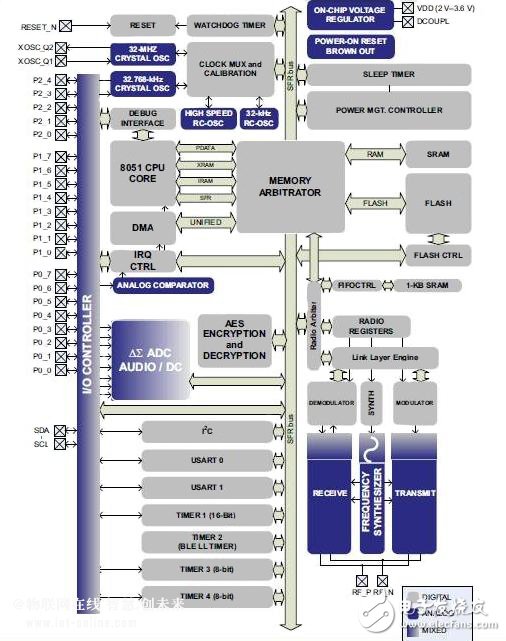
6&TImes; 6mm SOC (Figure 2), integrates a wide list of other features and features, including an 8051 microcontroller, a native format and protocol stack, considerable memory, three timers, 23-day general purpose I / O (GPIO) pin, an eight channel a / D converter, a watchdog timer, a battery monitor, a temperature sensor, and I2C / SPI and UART interface. The goal of the equipment, but does not guarantee the global radio frequency regulations such as TPSI EN 300 328 and EN 328 (Europe), FCC CFR47 15 (USA), and STD-T66 (Japan).

Figure 2: Bluetooth Smart Soc for Devices The CC2451 family of Texas Instruments is highly integrated, with many features and functions that go beyond basic requirements to simplify design, reduce space, save energy, and reduce costs.
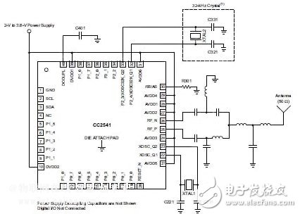
With IC, TI offers a range of product development tools such as the Evaluation Module Tool (CC2541EMK), a Mini Development Kit (CC2541DK-MINI), SmartRF Software and more. The typical application circuit CC2541 (Figure 3) shows the required external components.

Figure 3: In a typical application scenario, only a few external passive components need to provide full Bluetooth Smart CC2451 functionality.
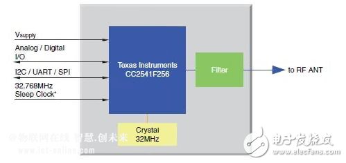
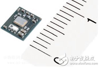
Even with this powerful and highly integrated Bluetooth integrated circuit, the success of this SOC's multifaceted challenge to their end product is more acceptable than many oem vendors. In these cases, a module such as TDKSESUB-PAN-T2541 provides an alternative (Figure 4). It uses the TI CC2541F256 SOC but is actually small (about 4.6 x 5.6 mm) because it is based on bulk dead, including crystal, RF filters, bypass capacitors, and other discrete component application circuits (Figure 5 ). The user must also add details of the size, type and location of the antenna that is compatible with the final product.

Figure 4: Despite the integrity of the CC2451 SOC family, some designers are reluctant to deal with any challenging rf circuit layout, rather than want a complete, certified SESUB-PAN-T2541 from TDK and other modules.

Figure 5: The fully enclosed SESUB-PAN-T2541 module square, approximately 5 mm, requires DC power and an external antenna, as well as software drivers and interface stacks.
The Internet of Things is a casually composed application component and market opportunity in a positive feedback relationship-ironically convenient mutual support, and engineers generally do not want to see the relationship. The necessary RF-connectivity components of the supplier are investing in new products to support applications and drive economic growth; in turn, application growth is leading to existing and new suppliers entering the market and generating new components. Particularly useful in the RF field, new components and software tools are needed to simplify the design challenges faced by designers when effectively interacting with new interactions and often mysterious world successes.
to sum up
An IoT node has three main functions: a sensor, a processor, and a connection interface, which is usually a wireless connection. Decide which wireless standard to use, if any, and then how to effectively implement it to closely match the challenges designers must face. There are technical, performance, power and cost trade-offs, as well as the choice to use basic integrated circuits, chip + reference designs, or completion modules, along with the depth of vendor software support, which is a key consideration for application areas. 
Audio Line Transformer,10W 6Ohm Audio Line Transformer,Audio Line Transformer 100V,Audio Line Transformer 70V
Guang Er Zhong(Zhaoqing)Electronics Co., Ltd , https://www.gezadapter.com