The x1 voltage amplifier or "buffer" is the standard building block for analog design. This article introduces the design of a high-performance discrete matched transistor buffer with a small number of components, and covers some details of optimizing its design.
In an era when a buffer can be easily implemented with an operational amplifier, why use discrete circuits? When high precision and minimum space are not particularly important indicators, a dual JFET amplifier with a part cost of 50 cents is sufficient to meet the performance requirements. It can provide a bandwidth of hundreds of MHz, an offset error of only 10mV or less, and a drift of 10μV/ oC or less. Through application innovation, discrete component circuits can also obtain good performance, even if the operational amplifier is out of date, it can still be used. The buffer can also be an important part of the design library.
Buffer amplifier circuit
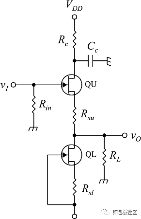
The design goal of the x1 voltage amplifier is to achieve such an ideal voltage amplifier: infinite input impedance, zero output impedance and linearity. In order to achieve high input impedance, use JFET instead of BJT, as shown in the buffer circuit in Figure 1.

Figure 1: In order to achieve high input impedance, use JFET instead of BJT.
Discrete JFET devices are available from multiple vendors, including:
·Linear Systems
· Fairchild (now ON Semiconductor)
·Philips (now NXP)
·Toshiba
·Vishay Siliconix
Although single package dual devices (such as 2N3958, 2N5196~2N5199, and 2N5564~2N5566, etc.) have advantages in heat tracking, in order to reduce costs, we still choose discrete JFET devices. The low-end dual devices cost about US$4.50 each, and the best ones are more than US$40. If you can afford the additional cost, you can choose expensive dual devices because their heat tracking performance is better than discrete JFETs.
Some of the discrete N-channel JFET alternatives required to design buffers include 2N5484~2N5486. The cost of 2N5485 is about US$0.20 each (when hundreds of units are purchased in bulk). The nominal design value of its drain current is within the specified range of 4~10mA, and the median value is IDSS = 7mA (IDSS is ID@VGS = 0V). In addition, two JFETs were selected for matching using the curve tracer. They can be manually classified into matching IDSS boxes. Each pair takes less than a minute and generates an additional cost of US$0.10 (calculated according to US labor costs).
Next, select some standard power supply voltages: VDD = +12V, VSS = -5V. These power supply voltages are common in desktop computers and instruments.
Offset voltage
The first design feature of the matched JFET is the static (dc) tracking of the matched transistor. If the gate of the bottom transistor QL is connected to its source, then VGS = 0V and the drain current is IDSS. If the same current flows through QU (with an open load), then because it is matched, its VGS is also zero, and there is no voltage offset between input and output.
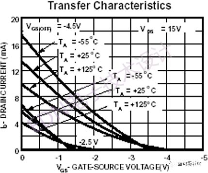
This wonderful design technique can also be improved by setting the JFET operating point to zero TC, where the thermal drift of VGS with a given ID is the smallest in the entire temperature range. For JFET, the zero-drift VGS is about 0.8V higher than the pinch-off voltage. The value of VGSZ is where the ID lines of various temperatures intersect. For 2N5485, this is approximately -1.2V, which is approximately 0.8V higher than the pinch-off voltage of approximately -2V. The curve of 2N5485 (Siliconix) is shown in Figure 2.

Figure 2: The graph of 2N5485 (Siliconix).
Using these values, Rsl = Rsu = Rs = 1.2V/5mA = 240Ω, with a tolerance of 5%. The voltage drop on Rsl is compensated in the waveform path by a similar voltage drop on the matching resistor Rsu. For better matching, the tolerance of these resistors can be 1%.
Thermal distortion
As the input voltage changes, the power consumption of the two JFETs also changes. Changes in power cause changes in silicon temperature, which can cause thermally induced electrical noise or "heat" in the amplifier's response. This "noise" is related to the waveform and is best viewed as thermal distortion. By setting the operating point (op-pt or bias) of the maximum power consumption of the JFET, the power consumption of the JFET can be minimized without changing the input (that is, at the op-pt point). The change in power (which we want to minimize) is the smallest near the peak power, where the derivative or slope of the parabola is the smallest.
Let the operating point of the JFET-the static bias current be I0. Then the power consumed by the upper and lower transistors is:

and:

Where vL is the load voltage on RL. The difference in power consumption is:

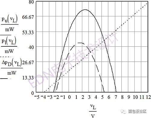
Figure 3 is a power consumption diagram compiled by MathCAD.

Figure 3: Power consumption diagram compiled by MathCAD.
When ΔpD is the largest, the power change with vL is the smallest, which is required to minimize thermal distortion. The vL value at the maximum differential power is:

Another voltage of interest is when pu and pl are equal. Solve vL when ΔpD = 0W:

In Figure 3, vL0 = 5.3V. Although the power consumption is matched at this output voltage, any change around this value will cause the change in ΔpD to be greater than the same change in vL near vL(max). Therefore, the preferred bias point is vL(max).
In Figure 3, vL(max) = 1.62V. However, given circuit parameters result in a static vL of 0V. In order to adjust the static voltage on the JFET, an additional series resistor Rc is added. Under normal circumstances, let the static output voltage be VL. Then set the vertex of the differential power parabola at VL:

Solve the value of VDD that meets the required conditions:

Then substitute VL and supply voltage VDD into the following equation:

In this design, Rc = 490Ω. Cc bypasses Rc, so that there is no significant voltage change at the drain.
Matching BJT buffer amplifier
JFET is better than BJT because of its high input resistance and low input bias current. However, for the same temperature coefficient (TC), the current matching of the JFET must be ten times better than that of the BJT. This is why the input offset specifications of JFET input op amps are usually worse than those of BJT. In short, BJT matches better than JFET.
If your buffer design does not require high input resistance, please use BJT instead. With the fixed base voltage of QL, the bias must be achieved in a slightly different way. This makes QL a current source that drifts with temperature due to VBE(T). The matched QU with similar drift has the same bias current and dynamic emitter resistance:

When ICL (=IEU) changes with temperature, the resistance remains constant. As the temperature increases, VBEL decreases and ICL increases. At the same time, reU increases with the thermal voltage VT, but the increased emitter current is compensated by reducing reU. The current TC from QL compensates for changes in re, which affects the buffer voltage gain.
The basic buffer stage introduced here can be improved by following the complementary BJT CC stage, which eliminates the be junction of NPN and PNP. If the matched NPN is connected in series with the QL source, it will compensate the subsequent NPN CC stage.
Upholstery And Decoration Staple
Zhejiang Best Nail Industrial Co., Ltd. , https://www.beststaple.com