I. Introduction
As early as the early 1990s, there were opinions that the Charge Coupled Device (CCD) was gradually becoming a "technical dinosaur". If you look at Sony's 2015 release, the prediction seems to make sense: Sony officially announced the end of the production CCD schedule and began receiving final orders. Although the industry has expected this to happen sooner or later, the release of Sony still shocked the professional imaging community. It is worth mentioning that many industrial or professional applications (the key markets for CMOS image sensors (CIS)) are still based on CCD sensor technology. What are the characteristics of CCD better than CIS, making it more attractive?
In the early days of development, CCD and CIS technologies coexisted; later CCDs were considered as high-end technologies capable of meeting stringent image quality requirements, while CMOS technology was still immature and subject to its inherent noise and pixel complexity. problem. During this period, image technology still dominated the analog structure, and the idea of ​​integrated image processing (system-on-chip SOC) has not been seriously considered. Based on Moore's Law, the shrinking of technology nodes has enabled SOC technology to rapidly expand and become more competitive from 2000. Now CIS continues to strive to improve optoelectronic performance, which is superior to CCD in many respects. If you use the "evolution" metaphor mentioned in the first article, you can actually regard CIS as a mammal that survives many natural disasters, and this evolutionary history is an epic story that spans 65 million years!
II. CCD and CMOS: homologous
The CCD works by converting photon signals into electronic packets and sequentially transferring them to a common output structure, which then converts the charge into a voltage. These signals are then sent to the buffer and stored off-chip. In CCD applications, most of the functions are performed on the camera's board. When the application needs to be modified, the designer can modify the circuit without having to redesign the image chip. In a CMOS image sensor, the operation of converting a charge into a voltage is performed on each pixel. CMOS image chips convert charge to voltage at the pixel level, and most of the functionality is integrated into the chip. In this way, all functions can be operated from a single power source, and the image can be flexibly read out according to the region of interest or window opening. In general, CCDs use NMOS technology to achieve performance through specific processes such as double-layer polysilicon, antiblooming, metal shielding, and specific starting materials covering each other. CMOS is based on standard CMOS process technology for digital integrated circuits, and then incorporates imaging functions (such as embedded photodiodes) according to customer requirements.
The general insight is that the production cost of a CMOS sensor is lower than that of a CCD, so its performance is also lower than that of a CCD. This assumption is based on market demand considerations, but other professional market opinions suggest that the technical level of the two is similar, and CCD may even be more economical. For example, large-scale major aerospace programs still use CCD components, not only because CCD achieves performance optimization at the process level under small batch and low-cost considerations, but also for long-term stable supply requirements. Similarly, high-end CCD-based solutions also have a mainstream share in the scientific imaging market, and there are some new products in the development phase. The situation is that dinosaurs have evolved into birds, and most of them provide excellent imaging capabilities...
CMOS has an improved system complexity because it basically embeds a System-On-Chip (SOC) structure such as analog-to-digital conversion, correlated double sampling (CDS), clock generation, and voltage regulators. Or post-image processing and other functions, which were previously available in system-level design. Today's CIS is typically produced in a 1P4M (1-layer polyester, 4-layer metal) process from 180nm to the recent 65nm, allowing the pixel design to incorporate very high conversion factors for easy column gain amplification. This makes CMOS optical feedback and light sensitivity generally better than CCD. Compared to CMOS, the CCD chip has better substrate bias stability and fewer circuits on the chip, so it has a more significant low-noise advantage, even reaching the level of no fixed-mode noise.
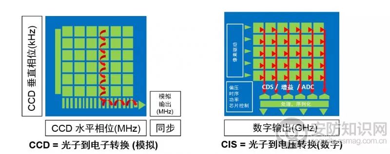
Figure 1 – CCD and CMOS structure comparison table
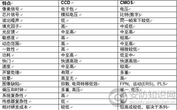
Table 1 – CCD-CMOS Features Comparison Table
On the other hand, CIS has a lower sampling frequency, which can reduce the bandwidth required for pixel reading, and thus the instantaneous noise is also small. The shutter exposes all pixels on the array at the same time. But with this approach, CMOS sensors take up more pixel space because they require extra transistors per pixel. In addition, each pixel of CMOS has an open-loop output amplifier, and the compensation and gain of each amplifier will change due to the difference in wafer process, making the high or dark unevenness worse than the CCD sensor. Compared with the CCD sensor of the same level, the CMOS sensor has lower power consumption, and the power consumption of other circuits on the chip is lower than that of the CCD optimized analog system chip. Depending on the amount of supply and considering the cost of the CCD to introduce external related circuit functions, the CMOS system cost may also be lower than the CCD. Table 1 summarizes the characteristics of CCD and CMOS. Some functions are beneficial to one or other technologies, so there is no need to completely separate the overall performance or cost. However, the real advantage of CMOS is the introduction flexibility through system-on-chip and its low power consumption.
I. Common misconceptions about noise performance
The bandwidth of the video imaging chain must be carefully adjusted to minimize readout noise during the digitization phase. However, this bandwidth must also be large enough to prevent other defects in the image. This usual practice also applies to CCD and CMOS. The minimum threshold for bandwidth is determined by the time it takes for the sample to reach a level close enough to the ideal level. Induced errors should be at a negligible level close to the Least Significant Bit (LSB). To determine the bandwidth you need, you can apply the following guidelines:

The amplification chain bandwidth fc, the signal frequencies fs and N (ie, the ADC resolution) are placed in the calculation formula. For example, when N=12, the value is:

The noise is most caused by two factors: 1/f flicker noise and thermal noise (see Figure 2). Flicker noise is a common noise in nature, and its spectral density is related to the Earth's rotation speed, seabed currents, weather and climate phenomena. The study shows that the flash rate of a normal candle is 1/f. Among the elements of the MOS device and the amplification chain, the flicker noise is a defect caused by the technical process error, causing the charge to be trapped in the gate oxide. Charges enter and exit these "traps", causing the current in the transistor channel to be unstable, so it is also called "random telegraph noise" (RTS). The Lorentzian mathematical model can be used to describe the resonant behavior of each "trap", and the sum of the models (ie, the sum of all the "traps" of the MOSFET channel surface range) is displayed on the 1/f spectrum. Complete the spectral density of the specific noise. The results show that the 1/f amplitude is inversely proportional to the surface area of ​​the MOSFET channel—not completely intuitive.
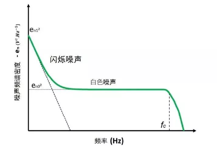
Figure 2 – Spectral noise density
To remove or reduce amplifier common-mode differences on CIS, floating-point reset noise and even transistor technology dispersion, video channels typically integrate a correlated double-sampling (CDS) stage. This element converts the video signal transfer function according to the following formula:

In the formula, fs is the sampling frequency and n is the CDS factor (usually n=2). As shown in Figure 3, depending on the sampling frequency, this filtering removes the 1/f noise frequency component more or less, especially when the sampling frequency fs is high (in other words, the action of the charge in and out of the "trap" will Slower than the CDS frequency). The low pass filter of the HCDS filter combined with the amplification chain can be simplified to an equivalent band pass filter as shown in FIG. The eqBP1 in the figure corresponds to a first-stage bandpass filter. Here the noise spectrum function of eqBP1 is divided by 2 to obtain an equivalent integrated noise power with an HCDS function. eqBP2 is the notch estimate for eqBP1. To achieve integrated noise power, the upper and lower limits of eqBP2 are multiplied by the following equations:

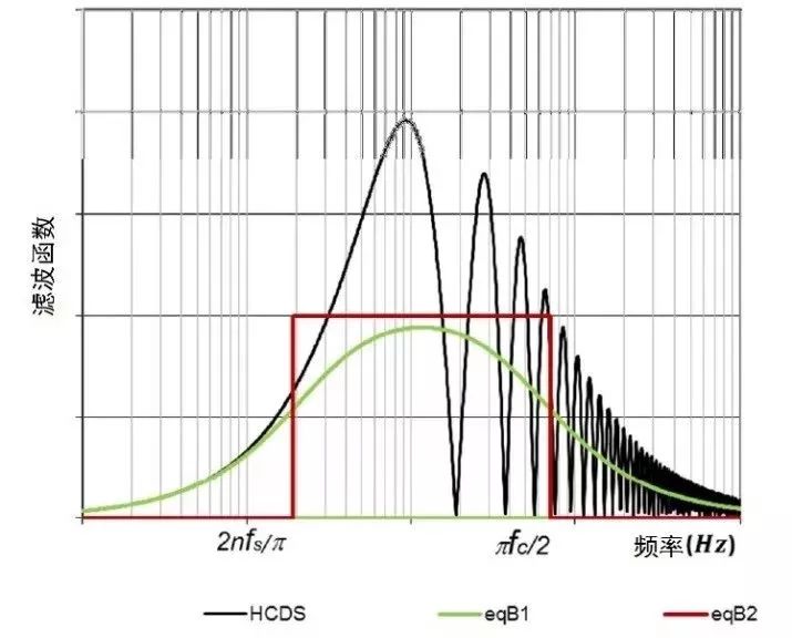
Figure 3 – Noise Filter Function
In the general situation shown in Figures 2 and 3, the noise performance can be shown in the following equation:

Combining equations (1) and (4) yields an estimate of the overall integrated readout noise as follows:

The calculations are verified to match the numerical simulation results. The readout noise of the CCD can reach very low levels, suitable for astronomical or scientific imaging, and the readout frequency of these applications can be very low. The system design contains electronic elements with minimal bandwidth to avoid integration into the unstable clock of the signal. In these applications, the 1/f component of the noise dominates. In high speed video applications, high noise makes the signal to noise ratio significantly worse. The specific noise representation status data recorded from a number of different CCD video cameras confirms the theory. The columnar parallel readout layout of the CMOS image sensor (see Figure 1) offers advantages in this regard. The threshold readout frequency is divided by the number of columns and compared to the CCD value. Here, the read noise of the CIS is mainly dominated by the 1/f value. This helps to further improve the imaging performance of CMOS technology. Recent results show that CIS can provide excellent noise performance in the range of 1E- or lower.
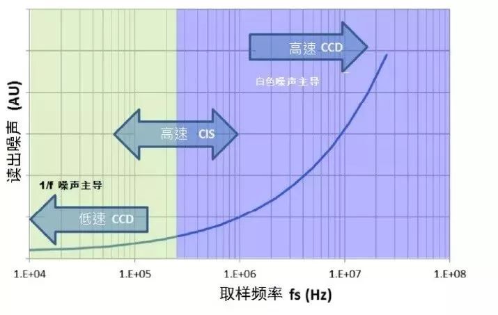
Figure 4 – Readout noise as a function of fs
II. MTF and QE: pillars of image quality
Quantum efficiency (QE) is a factor that directly affects the photoelectric performance of an image sensor, because any loss of photoelectric conversion efficiency directly reduces the signal-to-noise ratio (SNR). Its effect is two-fold, because when shot noise (the square root of the signal) is the main source of noise, QE is not only the divisor (signal) of the signal-to-noise ratio, but also the divisor (noise). Above this point, CCD and CMOS are at the same level, but CCD has accumulated many years of technical process optimization in QE improvement, and the development of QE in CIS is relatively late. Based on the physical properties of the silicon species, longer wavelengths can penetrate the photosensitive conversion zone, so thick epitaxial materials are used to increase the QE of the red and near infrared wavelengths. According to the Beer-Lambert law, the absorbed energy is exponentially related to the thickness of the medium. High-end applications CCDs have advantages by using thicker silicon materials and back side illumination (BSI) processes to restore high-bandwidth QE and near infrared (NIR) sensitivity.
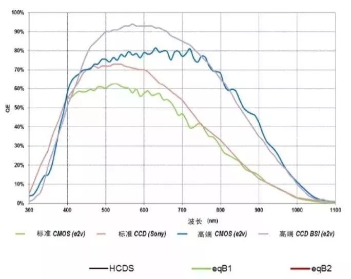
Figure 5 – QE Indicator
Interline transfer CCD (ITCCD) is based on a specific production process that introduces a so-called "vertical overflow drain" (VOD) or "vertical antiblooming" (VAB) function. VAB was developed in the early 1980s with very good performance, but the disadvantage is that it reduces the red feedback and rejects the NIR part of the spectrum.
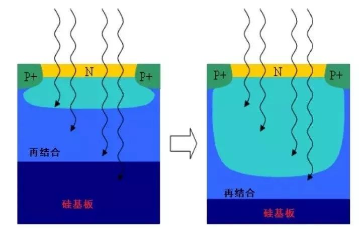
Figure 6 – Deep exhaustion method
For this reason, ITCCD cannot benefit from BSI. The high-end CCD does not have this limitation because it uses a vertical anti-halation process. CMOS also has the same feature: on a thin sensing layer, because the charge does not penetrate between pixels, there is no disadvantage of crosstalk. The result is that both the ITCCD and the standard CIS can achieve good spatial resolution or modulated transfer function (MTF). To increase the NIR portion and sensitivity, it is necessary to significantly increase the material thickness, but thick materials will increase the photoelectric crosstalk, resulting in MTF attenuation. Image quality is the combined result of MTF and QE (the so-called Quantitative Quantum Efficiency, DQE), so both airspace and time domain factors must be considered. Figure 6 shows a deep depletion photodiode that recovers MTF using a silicon doping method. In general, CIS is produced using common techniques similar to integrated circuits (especially DRAM/memory processes), so the specific process recipes described above are not involved. However, recent technical research articles show specific process introductions for CIS that can achieve excellent QE improvements and even relatively close to the high-end CCD level (see Figure 5) [9][10]. The latest CMOS technology trends are leaps and bounds, introducing technologies such as light guides, deep trench isolation (DTI), buried microlenses, and embedded chips containing pixel transistors in the photosensitive range.
III. Inherent defects
"Pinned photodiode" (PPD) or "hole accumulation diode" (HAD) was originally developed to eliminate delay and transfer all charge from the photodiode to the ITCCD register. A major development in CMOS image sensors was the introduction of ITCCD photodiode structures in the early 2000s, as shown in Figure 7. In CMOS, the pixel structure is mostly represented by the number of transistors per pixel. Most CMOS image sensors tend to use an electronic rolling shutter, which facilitates integration and can be implemented with as little as three transistors (3T). Despite the simple structure, the 3T pixel structure has the disadvantage that the pixel generated from the kT/C (or temperature) noise generates large time domain noise and cannot be easily eliminated.

Figure 7 – Comparison of ITCCD and 5T CMOS images
Embedded photodiodes were originally introduced to CIS to remove noise from floating diffusion resets and later introduced into four-transistor pixel (4T) structures. The 4T structure performs correlated double sampling (CDS) to eliminate reset transient noise. This structure also allows the transistor to share a layout between pixels in order to reduce the number of effective transistors per pixel to two or less. It turns out that the number of transistors per pixel is reduced, and more range can be vacated for the photosensitive portion or fill factor to more directly couple light to the pixel. However, as shown in Figure 8, ERS causes more image distortion when capturing video or images that contain fast motion. The PPD will work at the second level for global shutter (GS) capture. It removes ERS artifacts and further eliminates time domain noise, dark current, and fixed pattern noise. The function of the fifth transistor (5T) close to the PPD is to eliminate excessive charge and adjust the integration time of the overlap mode (readout during integration).
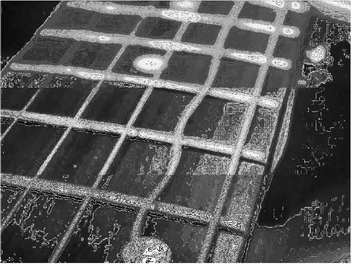
Figure 8 – Image 瑕疵: CMOS ERS Deformation
The global shutter (GS) mode is generally used with ITCCDs, but in some cases it is sensitive to diffuse appearance.
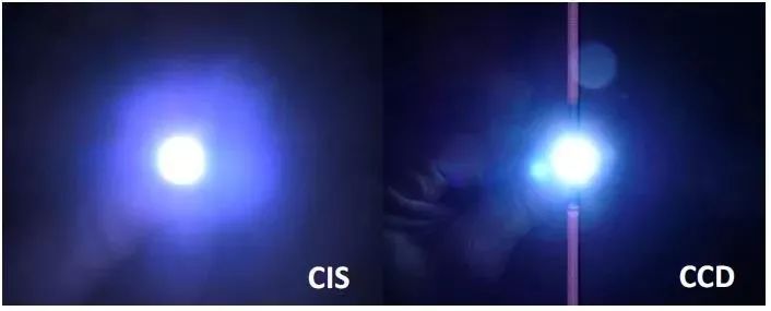
Figure 9 – Image 瑕疵: CCD dispersion
Dispersion is the appearance of a charge transfer, which produces a straight line on the image as shown in Figure 9. This is especially noticeable on high-contrast images, but it should not be confused with similar halos. The most common solution is to introduce a frame-interline transfer (FIT) CCD structure, and FIT also has the advantage of a higher video rate. The dispersion parameter equivalent to CMOS is Global Shutter Efficiency (GSE), sometimes called parasitic light sensitivity (PLS), which is the sensitivity ratio corresponding to the sensing node to the photodiode. The GSE of ITCCD is generally between -88dB and -100dB [13], and in CMOS it is -74dB to -120dB or even -160dB for 3D laminate [14]. The use of advanced custom pixel microlens (such as zerogap) can achieve significant differences in improving the sensitivity of wavelength feedback to reducing the fill factor loss caused by diodes on CMOS pixels. It is also a major factor in improving GSE performance.
IV. The future of CMOS imaging technology
CCD technology is particularly suitable for the field of time delay integration (TDI). The introduction of TDI (integration and accumulation of electronic synchronization during scanning of a scene) is relatively straightforward and requires only one charge transfer device. This technique was originally used to maximize signal-to-noise ratio and then used in CIS CCDs to preserve good image definition (MTF). In recent years, attempts to accumulate multiple signals in analog regions (voltage) or digital regions have opened up new directions for CMOS TDI. The low noise and high sensitivity performance of the CCD delay integration structure is popular both in space ground observation and in machine vision. However, the most anticipated development at present is based on CMOS technology, but with the advantages of CIS CCD and the technology of charge transfer register combined with line ADC converter. Despite significant advances, the sensitivity of CMOS image sensors is limited by readout noise in applications where light is very weak (such as in environments with only a few tens of micro-lumen). The EMCCD, which uses electron multiplier technology, shows great potential for noise reduction and is therefore receiving the attention of the scientific imaging market. In general, just as CCDs are replaced by CMOS sensors, EMCCD has the potential to move toward electronic multiplying CMOS (EMCMOS). Like EMCCD, EMCMOS plans to improve image quality in very weak light applications to match scientific or surveillance applications. CMOS technology helps to achieve smaller, smarter systems and lower power consumption to reduce the cost of production. (the so-called SWAP-C method). The principle of electron multiplication is to gain a signal before any noise is added to the sense chain, so that the noise is spread by the gain to improve the signal-to-noise ratio. Based on the CCD principle, the signals are transmitted in the form of an electronic packet, and then each pixel is multiplied together before reading. The CMOS signal is in the voltage domain, so multiplication must be done before the source follower adds noise to the signal and transfers it to the floating point.
With the popularity of 3D imaging, information on object depth is required, and Time-Of-Flight (TOF) technology comes in handy. The principle of TOF is to set up an artificial pulse light source on the sensor plane and emit it, and then use the feedback reflection band for correlation function calculation to get the distance. This technique was first proposed in the "locked" CCD in 1995. The application of TOF in CMOS is inspired by CCD pixels. Another method is to measure the depth using a Current Assisted Photonic Demodulator (CAPD). Both methods enable mass production of industrial 3D sensors and enable a range of applications such as counting numbers, safety monitoring, metrology, industrial robotics, gesture recognition, and advanced automotive driver assistance systems (ADAS). This is a typical example of the CCD technology-derived ideas that have been successfully over-provisioned to CMOS for further large-scale introduction of industrial applications.
The introduction of CMOS technology has also spawned new applications. For example, CCD was similar to vidicon tubes in the professional camera field in the 1980s. The single photon avalanche diode (SPAD) was originally developed as a photomultiplier tube (PMT). ) Solid state replacement products. The SPAD is basically a pn junction that is biased in accordance with the back pressure in the breakdown mode in the so-called Geiger mode. However, this structure is very unstable and any energy change will cause an avalanche effect. This feature is used for single photon sensing. By introducing a simple capacitive component between the SPAD and the input voltage, using the passive suppression principle to open and close the avalanche, or using the embedded MOSFET channel to initiate the active suppression principle for the same purpose. This makes it possible to create digital signals that represent quantum events. According to the principle, SPAD is a simple structure based CMOS technology that does not require a special process for image sensors. However, because it requires complex circuits, the work of SPAD arrays is more complicated. As with the arrival of photons, SPAD triggers and event counts are defined as asynchronous. CMOS technology is therefore the best choice. For example, this enables the scanning pixel array to be activated very quickly to confirm the converted pixels. These frames are combined to create a video sequence.
V. Summary
Some early articles claiming the end of the CCD era have been regarded as prophecies, but the actual transition time is much longer than expected. On the other hand, the types and innovations of image structures developed for CMOS image sensors have greatly surpassed previous imaginations. These innovations have become viable as transistor etch processes have shrunk and CMOS production technology has evolved. In addition to price, large industrial imaging manufacturers continue to compete in optoelectronic performance. Nowadays, users are not only taking pictures, but taking important moments in their lives, and expect to take perfect photos regardless of any light conditions. Industrial applications have also benefited from these general improvements due to these improvements. More and more vision systems are also adjusting their image sensor requirements based on consumer market trends, and image reduction is an example. High-speed processing is also an important economic factor because it can increase the output of high-cost production machines and automate processes and inspections. New applications are pushing the sensor to performance limits and not allowing more noise in the image, driving single-photon imaging. In addition to simple photography and display, 3D Augmented Reality technology also exhausts all the potential of CMOS technology to provide an alternative visual space experience. Like the main species on Earth, CMOS sensors have evolved greatly and adapted to their surroundings.
Blade Fuse is a kind of current fuse, when the circuit current exceeds the fuse rated current of 2 times in a few seconds when the fuse will play the role of circuit protection. Widely used in equipment circuit protection standard for foreign and domestic automobiles and trucks. Readily identifiable and easily replaced, this fuse can be specified for a variety of low voltage electronic Applications.
Harness Component
Dongguan YAC Electric Co,. LTD. , https://www.yacentercns.com