First, the circuit and working principle
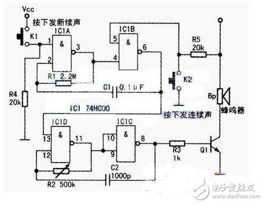
The circuit is shown below. The 74HC00 is a four-two input NAND gate.

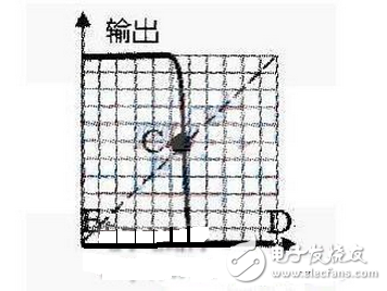
If the input of the two input terminals is connected to the high level of the NAND gate, or the two inputs are shorted, the output is inverted with the remaining one input or two shorted inputs, which is equivalent to one. inverter. In the circuit shown below, set the 1 pin of IC1A and the 5 pin of IC1B to be high level (K1 is pressed, K2 is turned off), then IC1A can be regarded as 2 pin input 3 pin output, which can be regarded as IC1B4 pin input 6 The inverter output of the pin has the transmission characteristics as shown on the right. Due to the negative feedback of R1, if the voltage of pin 2 is low and the pin 3 outputs high voltage, the level of pin 2 is pulled high by R1; if the voltage of pin 2 is high and the output of pin 3 is low, then pin 2 is powered by R1. The flat pull is low and the result compromises at the center point C. The output is 100% fed back to the input, which is equivalent to folding the lower left triangle part to the upper right corner according to the dotted line. The intersection C of the dotted line and the transmission characteristic is the operating point of the inverter, which is approximately equal to 1/2 VCC. Point C is located at the center of the steep slope of the transmission characteristics. In this example, the 74HC00 input changes by 1mV and the output changes up to 1V.
Since the IC13 pin and the 4-pin are pressed, the signal output by the 6-pin is in phase with the 2 pin but the amplitude is enlarged. In the figure, C1 plays a positive feedback role. As long as the voltage of the 2 pin has slight fluctuations, such as increasing 0.1mV, the voltage of the 3 pin is reduced by 100mV, and then the IC1B is inverted, and the output voltage of the 6 pin is increased by more than 1V. This voltage change is sent back to the 2 pin through C1, so that the voltage of the 2 pin is Continue to rise until VCC + 0.7V. At this time, the protection diode inside IC1 is turned on, so that the input voltage cannot be high, and the operating point of the inverter stops at point D on the right. Point D is on the horizontal line of the transmission characteristic, and the input change hardly affects the output. At this time, pin 2 of IC1 is high level, pin 3 is low level, and pin 6 is high level. Resistor R1 is connected between pins 2 and 3. The 3 pin is the output end, the internal resistance is very low, the 2 pin is the input end, and the internal resistance is extremely high. The difference between the high and low 3 causes the direction of the current I on R1 to be as shown on the left, the initial voltage of the discharge is VCC + 0.7V, and the final voltage of the discharge is 0V.

The actual discharge to the point C (1/2 VCC) stops. The discharge from VCC+0.7V to 1/2VCC requires about 1.1R1C1=1.1&TImes; (2.2&TImes;l0(6))&TImes;(0.1&TImes;10(-6)≈0.25s.
At this time, the 2 feet become lower, after IC1A inverting amplification → 3 feet become high → IC1B inverting amplification → 6 feet quickly going low → C1 → 2 feet. The positive feedback continues until the 2-pin voltage drops to -0.7V. At this time, the protection diode inside IC1 is turned on, so that the input voltage cannot be low, and the operating point of the inverter stops at point E. Point E is on the horizontal line of the transmission characteristic, and the input change hardly affects the output. The state at this time is 2 low, 3 high, and 6 low. R1 charges C1. The charging start voltage is -0.7V and the final charging voltage is VCC.
Charging from 0.7V to 1/2VCC requires about 1.1R1C1=0.25s, then stop charging, enter positive feedback, and turn to operating point D. In fact, the circuit works in the D, E state for a long time, the time after C is very short, so the output is a square wave, a cycle of about 0.5s. The square wave has more harmonics than the sine wave and sounds more pleasant. The output signal of many music pieces is composed of equal-amplitude square waves of different frequencies. If the amplitude can change with the beat, it is better to listen. Similarly, IC1C's (13) pin = high, IC1D9, 10 are connected in parallel, can also be regarded as two inverters, generating a square wave oscillation with a period of 0.5ms. That is 2kHz. Because the resonant frequency of the buzzer is about 2 kHz, the electrical conversion efficiency is the highest, which sounds the loudest.
When the capacitor is selected at 1000pF, the resistance is about 250kΩ. In the figure below, the 500kΩ potentiometer is adjusted to the center position to find the maximum volume. R2 can also be used with 240kΩ ~ 270kΩ fixed resistors.

Because the resistance of the buzzer is about 40Ω, the output impedance of IC1 is about 1kΩ, so IC1 can't directly drive the buzzer, so it needs to be amplified by Q1. IC1C8 pin output high level 3V, Q1 base turn-on voltage is 0.7V, R3=1Ω, Q1 base current is (3-0.7)/1k=2.3mA, Q11 amplification is 50, collector current is 115mA. The 40Ω buzzer is driven by 70mA and the voltage at both ends is 2.8V. So where is the current of 115-70=45mA going? The Q1 amplification factor is 50, which means that Q1 is in the linear amplification area Ic/IB, and the saturation region, IG/IBF drops, when the tube pressure drop of Q1 is very low.
Non-logical control: IC1A's 1 pin is normally grounded through R4, 3-pin output is constant high, 4 feet = 3 feet, and 6-pin output is constant low. (13) Foot = 6 feet = low, 8 feet are low, and the buzzer does not sound. The entire circuit consumes a small amount of electrodes.
After K1 is pressed, (13) is high level, IC1D and IC1C generate 2Hz square wave, control IC1D (13) pin, (13) pin is high level, IC1D, IC1C generate 2kHz square wave is driven by R3, Q1 Buzzer; When the (13) pin is low, IC1D and IC1C stop, 8 pin outputs low level, and Q1 turns off. Thus, the buzzer emits an intermittent beep twice per second. The IC1B5 pin is connected to the high level through R5 and works normally. After K2 is pressed, the 5 pin is low, and IC1A and IC1B stop vibrating. (13) Feet = 6 feet constant height, the buzzer emits a continuous hum.
Second, the assembly of the general circuit board
Regardless of the number of components in the assembly, carefully plan before inserting components on the circuit board, and try to avoid staggering the wires.
As shown in the figure below, the pin arrangement of IC1 is counterclockwise from the notch, and the lower 7 feet are 1 to 7 feet, R1 is close to 1 to 3, C1 is close to 6 and 7 is ground, 7 The foot is close to the E pole of R4, K2, and Q1. The upper 7 feet are (8)~(14) feet, R2 is close to (13)~(11) feet, C2 and R3 are close to 8 feet, Q1's B pole is close to R3, and BP is close to Q1's C pole. After this layout, the IC1 is centered, and the upper and lower sides are barely connected on the plane of the general-purpose circuit board by bare copper wires or resistor pins, and the wires can be basically not staggered. When checking, it is also centered on IC1, one foot and one foot.
Third, debugging components
After all the installation is completed, it is not busy to test the power. First, an ammeter is placed between the power supply + and the test board VCC. Under normal circumstances, the current is extremely small. If the current is greater than 500μA and unstable, it indicates that the input terminal is suspended or soldered. It can be checked that the human body touches the metal part of the screwdriver, and the head of the screwdriver is sequentially touched with the screwdriver head. If the current changes significantly, it indicates that there is a problem with the connection of the foot. If the current is normal, put the ammeter in the 100mA (200mA) block, press the K1 current to change without ringing, check R3, Q1, BP; press K1 current is small and not loud, check IC1.
1. Check BP, use the tweezers to short-circuit the C and E poles of Q1, the current changes, and the buzzer should have a "card-bar" sound. If not, the BP is broken or the line is not connected.
2. Check the transistor, connect the VCC or ground with the tweezers near the IC1 end, and connect it back and forth. The buzzer should have a "card-bar" sound. If not, the transistor is broken, connected, or the line is not connected (the short circuit usually does not damage the IC).
3. Check IC1, press K2, use the digital multimeter to measure the voltage, and IC1's (8)~(12) feet should be neither high nor low. For example, in the case of a 3V battery, the measured value is about 1.5V. If 8 is constant low, (9), (10), (11) feet are always high, if (13) is high, it means that K2 is pressed, and (12) is low, indicating that R2 negative feedback does not work. Short circuit (11), (12) feet with red pen, black pen grounding, voltmeter display is not high or low, R2 may be soldered. If the (13) pin is low, it means that K2 does not work, check 6 feet and 5 feet. 5 feet high, indicating that switch K2 is bad or not connected. 6 feet, 5 feet are low, indicating that the IC is bad or the solder joint is shorted to the ground. When K1 is pressed, the 6-pin voltage reading is unstable. After a while, it is small, indicating that the 2Hz oscillation is normal. If it is constant or low, the red meter pen can be short-circuited with 2 and 3 feet to check the fault. The detection method of K1 pressing and so on.
This is a kind of functional e-cigarette - relaxing e-cigarette that makes you relax and calm down. Of course, it doesn't contain nicotine.
The effect will be better to take a few deep breaths after smoking this relax electronic cigarette. Moreover, it is small in size, simple in appearance,
and easy to carry.
We are China leading manufacturer and supplier of Disposable Vapes puff bars, relax vape pen,relax e-cigarette kit,
relax disposable vape, and e-cigarette kit, and we specialize in disposable vapes, e-cigarette vape pens, e-cigarette kits, etc.
relax vape pen,relax e-cigarette kit,relax disposable vape, relax e-cigarette vaporizer, relax bar vape
Ningbo Autrends International Trade Co.,Ltd. , https://www.mosvapor.com