2. High speed gate drive circuit
1 bootstrap gate drive technology
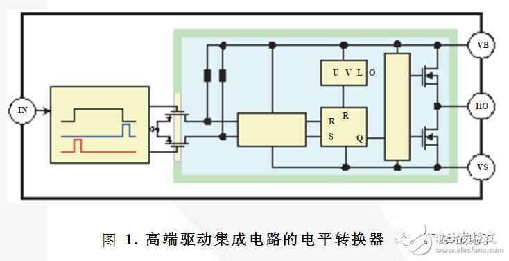
This section focuses on the requirements of bootstrap gate drive circuits for power MOSFETs and IGBTs in power switching applications with different switching modes . When the input level does not allow high-type N-channel power MOSFET or IGBT gate driving circuit direct use, we can consider bootstrapped gate drive technology. This method is used as the gate drive and bias circuit associated with, those two are the source of the main switching device as a reference electrode. Driving circuit and the bias circuit in the device with respect to the source voltage swings between two inputs. However, the floating driver circuit and its bias circuit can be implemented by a low pressure, because the input voltage is not applied to these circuits. The drive circuit and the ground control signal are connected through a level shifting circuit. The level shifting circuit must allow for a high voltage difference and a certain capacitive switching current between the floating high side and grounded low side circuits . The high voltage gate drive ICs are separated by a unique level shift design. In order to maintain high efficiency and power consumption can be managed, the level shifter circuit during the main switch is turned on, it can not absorb any current. For this case, we often use a pulsed latch level shifter, as shown in Figure 1.
2 bootstrap drive circuit works
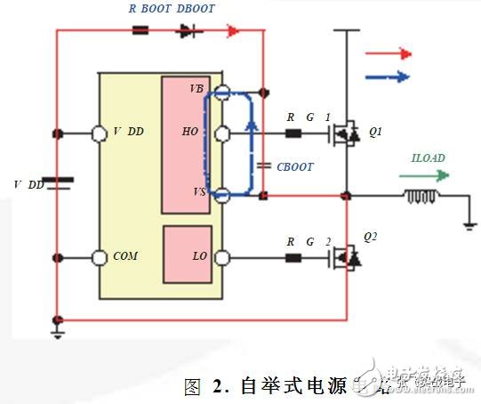
Bootstrap circuit in the high voltage of the gate driving circuit is useful, as it follows the principle of work. When V S drops to IC supply voltage V DD or pulls down to ground (low-side switch turns on, high-side switch turns off), power supply V DD passes bootstrap resistor, R BOOT , and bootstrap diode, D BOOT , bootstrap Capacitor C BOOT to charge, as shown in Figure 2. When V S is pulled to a higher voltage on the high side switch, a V BS of the bootstrap capacitor charging, this time, the floating power supply V BS, the bootstrap diode is reverse-biased, rail voltage (low-side switch is turned off , high-side switch oN) and IC power supply voltage V DD, is separated away.
3 shortcomings of bootstrap circuit
Bootstrap circuit has the advantage of simplicity and low cost, but it also has some limitations.
And the duty ratio of on-time is limited by the bootstrap capacitor C BOOT, refresh charge required time limit.
The biggest difficulty with this circuit is that when the switching device is turned off, the negative voltage of its source causes the load current to suddenly flow through the freewheeling diode, as shown in Figure 3.
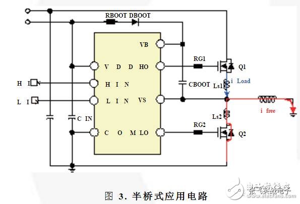
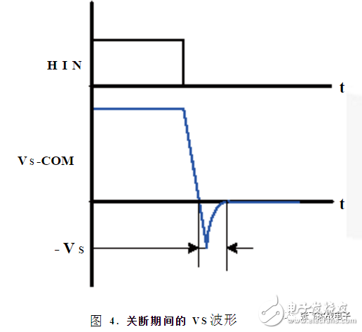
The negative voltage output terminal of the gate driving circuit will cause trouble, because it directly affects the source driving circuit or a PWM control IC pin V S, may obviously certain internal circuitry down to the ground below in FIG. 4 is shown. Another problem is that the conversion of this negative voltage may cause the bootstrap capacitor to be in an overvoltage condition.
The bootstrap capacitor C BOOT is instantaneously charged by the power supply VDD through the bootstrap diode D BOOT .
Since the V DD supply is referenced to ground, the maximum voltage generated by the bootstrap capacitor is equal to V DD plus the negative voltage amplitude at the source.
4 V S pin causes a negative voltage
As shown in Figure 5, the forward bias of the low-side freewheeling diode is one of the known reasons for lowering V S below COM (ground).
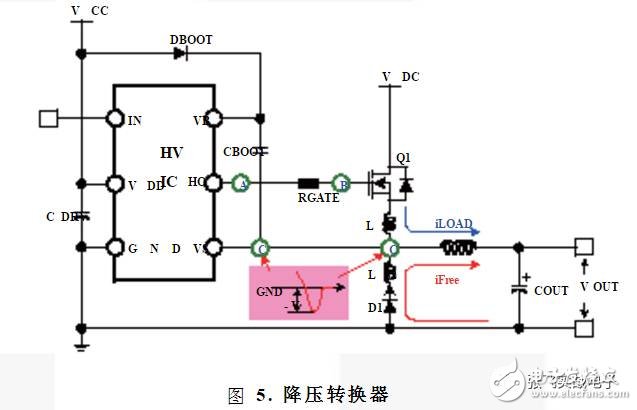
The main problem occurs during rectification commutation, just before the freewheeling diode begins to clamp.
In this case, the inductors LS1 and LS2 will be down to V S to the COM, or even more than normal steady state position as described above.
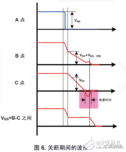
The amplification of this negative voltage is proportional to the parasitic inductance and the turn-off speed of the switching device , di/dt; it is determined by the gate drive resistor, R GATE and the input capacitance of the switching device , C iss .
The sum of Cgs and Cgd is called Miller capacitance.
Figure 6 depicts the voltage waveform during the turn-off of the high-side N-channel MOSFET.
5 V S pin voltage undershoot
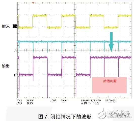
If the voltage undershoot amplitude exceeds a specified absolute maximum rating, the gate drive integrated circuit is damaged, or the gate drive integrated circuit temporarily latches the current state.
Figure 7 shows a high output signal with the input signal is not changed but the closing lock phenomenon, at this time, the half-bridge circuit external main switch is in the high and low short-circuit state.
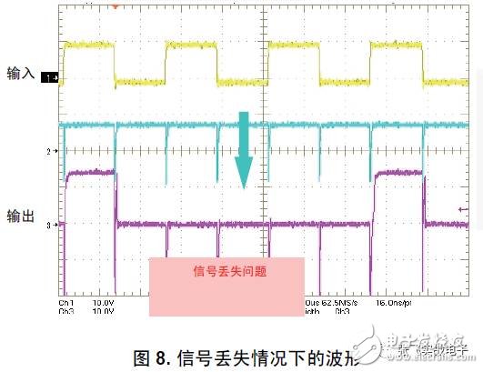
If the V S voltage undershoot does not exceed the specified absolute maximum rating, the gate drive IC will not be damaged. However, when V S is in the undershoot state as shown in Figure 8 , the high-side output does not respond to the input transition. In this case, high-level converter gate driving circuit is not affected by insufficient operating voltage headroom. It should be noted that most of the facts prove that the high-end is usually not necessary to change the state immediately after a switch action.
6 consider the blocking effect
The most complete high voltage gate drive ICs contain parasitic diodes that are broken down in the forward or reverse direction, which can cause parasitic SCR latchup. The end result of the latch-up effect is often unpredictable, ranging from device instability to complete failure. The gate drive integrated circuit may also be indirectly damaged by a series of actions after the initial overvoltage. For example, the latch output leads two simultaneously driven in a high state, causing cross-conduction, causing switch malfunction, and eventually the gate driver integrated circuit catastrophic destruction. If the root cause of the power converter circuit and / or the gate driving integrated circuit by destruction, this failure mode should be considered as a possible. Theoretical limit of the surface may be used to help explain a serious shortage of the voltage V S and thereby generating the relationship between the locking effect.
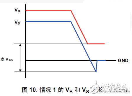
In the first case, the use of a "over the bootstrap circuit", V DD of the circuit is driven by a zero-ohm power supply, a diode is connected to the V B over through a, as shown in FIG. When a large current flows through the freewheeling diode, since di/dt is large, the V S voltage will be lower than the ground voltage. At this time, the risk of the latch, because the internal parasitic diode D BS gate driver, to the final V S V B along the direction of conduction, the voltage overshoot caused by the superposition of the V DD, so that the bootstrap capacitor is overcharged, 10 Shown.
For example: if undershoot V DD = 15V, V S exceeds 10V, forcing the floating supply voltage above 25V, the diode D BS danger of breakdown, thereby generating blocked.
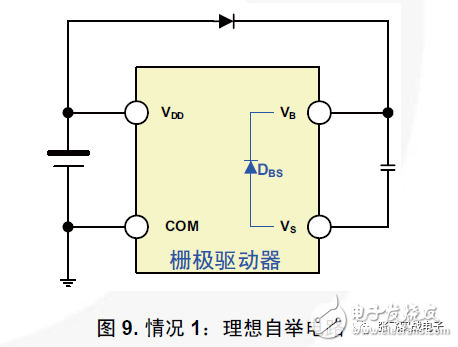
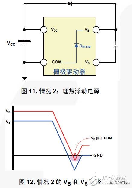
Virtual bootstrap supply is a floating power over Alternatively, as shown in FIG. 11, this time, V BS is in any case constant. Note that the use of a low-resistance auxiliary supply alternative bootstrap circuit can achieve this. In this case the maximum power V BS, if the overshoot exceeds V S data table (Datasheet) a predetermined pressure, the risk lockout occurs because the parasitic diode D BCM COM final end along the direction V B is turned on, as shown in Fig.
A practical circuit may be in between these two limits, the result is V BS voltage slightly increases, slightly lower than, V B V DD, as shown in Fig.
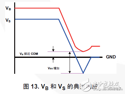
To be precise, any extreme situation is prevalent, as tested below. If V S overshoot duration more than 10 ns, is overcharged bootstrap capacitor C BOOT, then the high side gate driver circuit over-voltage stress destruction, as the V BS voltage exceeds the data table specified absolute maximum voltage (V BSMAX ). When designing a bootstrap circuit, its output voltage must not exceed the absolute maximum voltage rating of the high-side gate driver.
7 parasitic inductance effect
The amplitude of the negative voltage is:

In order to reduce the slope of the current flowing through the parasitic inductance as a function of time , the derivative term in Equation 1 is minimized.
For example: a 10 amps, 25V gate drive, which is parasitic inductance 100nH, if the switch within 50ns, then a negative voltage spikes between V S and ground is 20V.
3. Design process of bootstrap partsSelect a bootstrap capacitor
The bootstrap capacitor ( C BOOT ) is charged each time the low-side driver turns on and the output voltage is lower than the gate driver supply voltage ( V DD ). The bootstrap capacitor is only discharged when the high side switch is turned on. The bootstrap capacitor supplies power to the high-end circuitry ( V BS ). The first parameter to consider is the maximum voltage drop of the bootstrap capacitor when the high-side switch is on . The maximum allowable voltage drop (V BOOT) depends on the minimum gate drive voltage to be maintained (for high-side switch). If V GSMIN is the minimum gate-to-source voltage, the voltage drop across the capacitor must be:

among them:
V DD = the supply voltage of the gate driver;
V F = bootstrap diode forward voltage drop [V]
Calculate the bootstrap capacitor as:

Where Q TOTAL is the total amount of charge in the capacitor. The total charge of the bootstrap capacitor is calculated by Equation 4:

among them:
Q GATE = total amount of gate charge
I LKGS = switching gate - source level leakage current;
I LKCAP = leakage current of the bootstrap capacitor;
I QBS = quiescent current of the bootstrap circuit;
I LK = leakage current of the bootstrap circuit;
Q LS = charge required by the internal level shifter for all high voltage gates
Polar drive circuit, the value is 3nC;
t ON = high end on time; and
I LKDIODED = leakage current of the bootstrap diode;
The leakage current of the capacitor, and only in the use of electrolytic capacitors, it needs to be considered, otherwise, can be ignored.
2 choose bootstrap resistance
When using an external bootstrap resistor, the resistor R BOOT brings an extra voltage drop:

among them:
I CHARGE = charging current of the bootstrap capacitor;
R BOOT = bootstrap resistance; and
t CHARGE = charging time of the bootstrap capacitor (low-side conduction time)
The resistance value (typically 5 ~ 10 Ω) can not be too large, otherwise it will increase the time constant of V BS. When calculating the maximum allowable voltage drop (V BOOT), must be considered bootstrap diode voltage drop. If the voltage drop is too large or the circuit can not provide a sufficient charging time, we can use a fast or ultra-fast recovery diode recovery.
For example, when using an external bootstrap diode, estimate the size of the bootstrap capacitor.
Gate drive
IC=FAN7382
Switching device
=FCP20N60
Bootstrap diode
=UF4007
V DD =15V
Q GATE = 98nC (maximum)
I LKGS = 100nA (maximum)
I LKCAP = 0 (ceramic capacitor)
I QBS = 120A (maximum)
I LK = 50A (maximum)
Q LS = 3nC
T ON =25s (f s =20KHz, duty cycle = 50%)
I LKDIODE = 10nA
If the bootstrap capacitor is on when the high side switch is on, the maximum allowable voltage drop is 1.0V and the minimum capacitance value is calculated by Equation 3.

The bootstrap capacitor is calculated as follows:

The voltage drop caused by the external diode is approximately 0.7V. Assuming that the capacitor charge time is equal to high on-time (duty ratio of 50%). According to different bootstrap capacitor values, use the following equation:
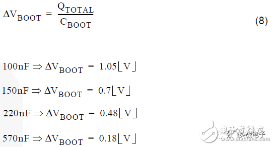
The recommended capacitor values ​​are 100nF ~ 570nF, but the actual capacitor value must be chosen based on the device used. If the capacitance value is too large, the charging time of the bootstrap capacitor is reduced, and the low-side conduction time may not be sufficient to make the capacitor reach the bootstrap voltage .
4. Consider the bootstrap application circuit1 bootstrap start circuit
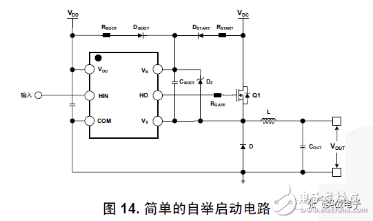
As shown in Figure 1, the bootstrap circuit is useful for high voltage gate drivers. However, when the source of the main MOSFET (Q1) and the negative bias node of the bootstrap capacitor ( C BOOT ) are at the output voltage, it has the problem of initializing and charging the bootstrap capacitor. At startup, the bootstrap diode ( D BOOT ) may be reverse biased, the main MOSFET (Q1) has insufficient turn-on time, and the bootstrap capacitor cannot hold the required charge, as shown in Figure 1.
In some applications, such as battery chargers, the output voltage may already exist before the input power is loaded into the converter. It may not be possible to provide an initial charge to the bootstrap capacitor (C BOOT ), depending on the voltage difference between the supply voltage (V DD ) and the output voltage (V OUT ). Assuming that there is enough voltage difference between the input voltage (V DC ) and the output voltage (V OUT ), the circuit consisting of the start-up resistor (R START ), the start-up diode (D START ) and the Zener diode (D START ) can solve This problem is shown in Figure 14. In this startup circuit, the startup diode D START acts as a secondary bootstrap diode that charges the bootstrap capacitor (C BOOT ) on power-up. After the bootstrap capacitor (C BOOT ) is charged, it is connected to the Zener diode D Z. In normal operation, this voltage should be greater than the driver's supply voltage (V DD ). The startup resistor limits the charge current and Zener current of the bootstrap capacitor. For maximum efficiency, the proper starting resistor value should be chosen so that the current is extremely low because the bootstrap path through the startup diode in the circuit is constant.
2 bootstrap diode series resistor
In the first option, the bootstrap circuit includes a small resistor, R BOOT , which is connected in series with a bootstrap diode, as shown in Figure 15. The bootstrap resistor R BOOT is used to limit current only during the bootstrap charge cycle. The bootstrap charge cycle indicates that V S falls below the integrated circuit supply voltage V DD , or V S is pulled low to ground (the low side switch turns on and the high side switch turns off). The power supply V DD charges the bootstrap capacitor C BOOT through the bootstrap resistor R BOOT and the diode D BOOT . The breakdown voltage (BV) of the bootstrap diode must be greater than V DC and the recovery time is fast enough to reduce the charge that the bootstrap capacitor feeds back to the power supply V CC .
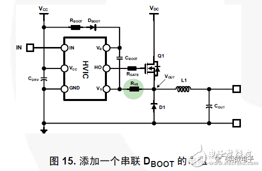
This is a simple way to limit the initial charge current of the bootstrap capacitor, but it also has some drawbacks. Duty cycle is limited by the time the bootstrap capacitor C BOOT refresh required charge, and startup problems. The resistance value (generally 5~10 Ω) should not be too large, otherwise the V BS time constant will increase . The minimum on-time, the time to charge or refresh the charge to the bootstrap capacitor, must match this time constant. This time constant depends on the bootstrap resistor, the duty ratio of the bootstrap capacitor and the switching device is calculated by the following equation:

Wherein R BOOT bootstrap resistor; C BOOT is the bootstrap capacitor; D is the duty ratio.
For example, R BOOT = 10, C BOOT = 1F and D = 10%; the time constant is calculated as follows:

Even if a reasonably large connecting the bootstrap capacitor and a resistor, the time constant may be increased. This method can alleviate this problem. Unfortunately, the series resistance can not solve the problem of over-voltage, and slowing the bootstrap capacitor recharging process.
3 VS and VOUT resistance
In the second option , add a small resistor RVS between V S and V OUT of the bootstrap circuit , as shown in Figure 16. The recommended value for R VS is around a few ohms.
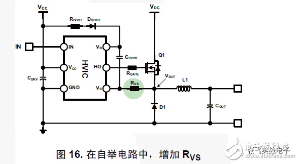
R VS not only as a bootstrap resistor also serves as the on-resistance and the off resistance, as shown in Figure 17. The bootstrap resistance, on-resistance, and turn-off resistance are calculated by the following equation :
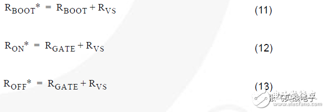
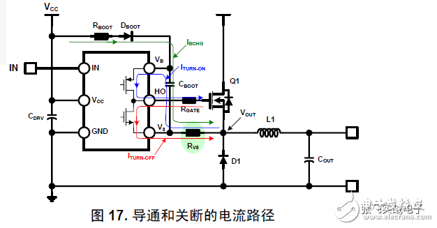
4 V S clamp diode and rearranged gate resistor
In the third option, the bootstrap circuit rearranges the gate resistor between V S and V OUT and adds a low forward voltage drop Schottky diode between V S and ground , as shown in Figure 18. Show. The voltage difference between V B and V S, should be maintained within a predetermined range of the absolute maximum ratings of the data table, and must conform to the following equation:
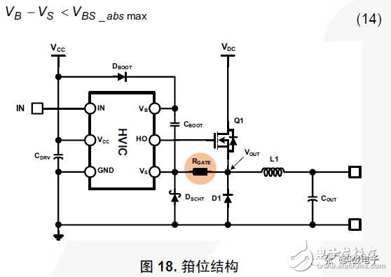
5 reset gate resistance; dual purpose
The gate resistor sets the turn-on and turn-off speeds of the MOSFET, limiting the current of the Schottky diode when the voltage at the source of the main switch is negative. In addition, the dual diodes connected to the ends of C BOOT ensure that the bootstrap capacitor does not overvoltage. The only potential danger of this circuit is that the charge current of the bootstrap capacitor must flow through the gate resistor. The time constants of C BOOT and R GATE slow down the capacitor recharge process, which may be a limiting factor similar to the PWM duty cycle.
The fourth choice, comprised between V S and V OUT, rearranging a gate resistor, and V S is placed between a clamp and the pressure device 19, a zener diode is arranged and 600V diode. Quantify the Zener voltage according to the following rules:
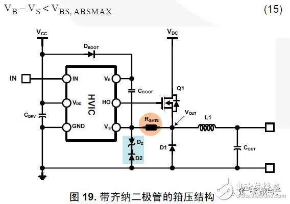
For each rated drive current, calculate the maximum gate charge Q G that can be switched within a specified time , as shown in Table 1.
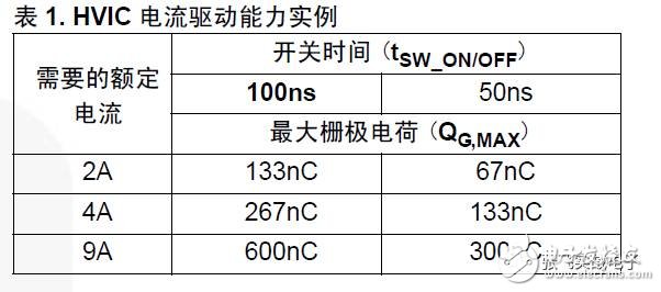
Description:
1. A single channel 4A HVIC, equivalent to a dual channel 2A HVIC!
For example, the switching time of 100ns is:
At 100KHz, 1% of the switching circuit switching period;
At 300KHz, the conversion circuit switching cycle is 3%;
1. The required nominal gate drive current depends on the number of gate charges Q G that must be moved during the switching time t SW_ON /OFF (because the average gate current during switching is I G ):

2. Maximum gate charge Q G , obtained from the MOSFET datasheet.
If the actual gate drive voltage V GS of the specification table the different test conditions, we can replace the value of Q G V GS curve used. Multiplying the value in the datasheet by the number of MOSFETs connected in parallel is the desired value.
3. t SW_ON /OFF indicates the required MOSFET switching speed. If the value is unknown, take 2% of the switching period t SW :

If the channel (VI) switching loss is dominated by switching (on or off) , the driver needs to be adjusted according to the conversion. For clamped inductive switches (normal), the channel switching losses for each conversion are estimated as follows:

among them
V DS and I D are the maximum values ​​for each switching interval.
4. The approximate current drive capability of the gate driver is calculated as follows
(1) Current capability (conduction)

(2) Current sinking capacity (shutdown)

among them:
Q G = V GS = V DD , the gate charge of the MOSFET;
t SW_ON/OFF = MOSFET switch on/off time; and
Experience factor = 1.5 (by delay and parasitics impact by the driver corresponding to the input stage)
6. Gate resistance design flowThe switching speed of the output transistors is controlled by the turn-on and turn-off gate resistors that control the turn-on and turn-off currents of the gate drivers. This section describes the basic rules for gate resistance by introducing the equivalent output resistance of the gate driver to achieve the desired switching time and speed. FIG 20 describes an equivalent circuit of the gate driver, and a current flow path is turned on and off during which includes a gate driver and a switching device.
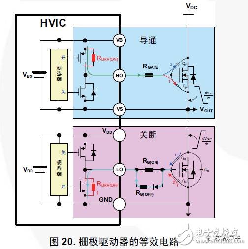
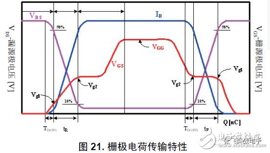
Figure 21 shows the gate of the switching device during turn-on and turn-off - charge-transporting properties.
1 quantize the on-resistance
The switching time t sw, selecting turn-on gate resistor R g (ON), the switching time to obtain the desired. The resistance values are determined when the switching time, we need to know the power supply voltage V DD (or V BS), the gate driver equivalent on-resistance (R DRV (ON)) parameter, and the switching device (Q gs, Q gd , and V gs(th) ).
The switching time is defined as the time it takes to reach the end of the platform voltage (which provides a total of Q gd + Q gd to the MOSFET ), as shown in Figure 21. The turn-on gate resistance is calculated as follows:

Where R g(ON) is the gate on-resistance and R DRV(ON) is the equivalent on-resistance of the driver .
2 output voltage slope
The turn-on gate resistance R g(ON) is determined by controlling the output voltage slope (dV OUT /dt) . When the output voltage is non-linear, the slope of the maximum output voltage can be approximated as:

Insert the deformation expression I g(avr) and sort it out:

Where C gd(off) is the Miller effect capacitor and is defined as C rss in the datasheet .
3 quantify turn-off gate resistance
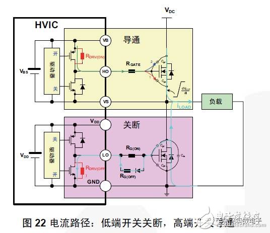
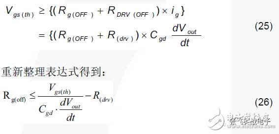
In quantifying the turn-off resistance, the worst case is when the MOSFET drain is off, an external action forces the resistor to rectify.
In this case, dv / dt output node, inducing an electric current through the parasitic through C gd, flow R G (OFF) and R DRV (OFF), shown in Figure 22.
Set forth below, when the output dv / dt turned on when accompanied by its cause, how to quantify the off resistance MSOFET, 22 shown in FIG.
For this reason, the impedance must be turned off according to the amount of the worst applications. The following equation correlates the MOSFET gate threshold voltage with the drain dv/dt :
4 design examples
Use Fairchild's MOSFET FCP20N60 and gate driver FAN7382 to determine the turn-on and turn-off gate resistance. The parameters of the FCP20N60 power MOSFET are as follows:
Q gs = 13.5nC, Q gd =36nC, C gd =95pF, V GS(th) =5V, V GS(th)MIN =3V
4.1 turn-on gate resistance
1) If V DD =15V, the required switching time is 500ns, calculate the average gate charging current:
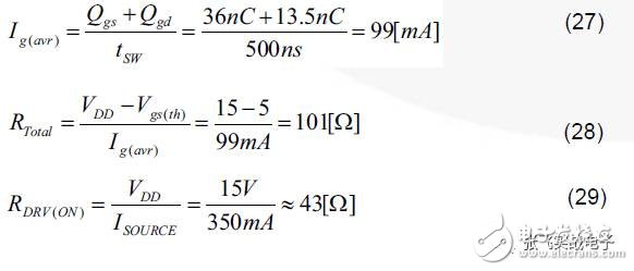
The on-resistance value is approximately 58 Ω.
2) If VDD=15V, dVout/dt=1V/ns, the total gate resistance is calculated as:

The on-resistance value is approximately 62 Ω.
4.2 Turn off the gate resistance
If dV out /dt = 1V/ns, the turn-off gate resistance can be calculated as:

1 gate driver power consumption
The total power consumption includes gate driver power and bootstrap diode power. The gate driver power consumption consists of static power and dynamic power. It is related to the switching frequency, high and low output load capacitance of the driver, and a power supply V DD.
Static power consumption because the power supply V DD to the low side driver of the quiescent current, leakage current and high-level conversion stage drive caused. The former depends on the voltage at the V S terminal, which is proportional to the duty cycle only when the high-side power device is turned on .
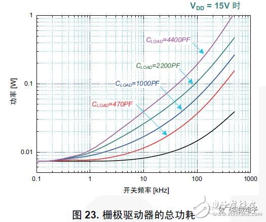
Dynamic power is defined as follows: For low-end drivers, there are two different sources of dynamic power . First, when the load capacitor is charged or discharged through the gate resistor , half of the energy entering the capacitor is dissipated on the resistor. Power consumption of the gate drive resistor, the inside and outside of the gate driver, and the switching power CMOS internal circuit. At the same time, the dynamic power consumption of high-end drivers also includes two different sources. One is because of the level shifting circuit, and the other is because of the charging and discharging of the high-side capacitor. Here, static power consumption can be ignored because the total power consumption of the integrated circuit is mainly the dynamic power consumption of the gate drive IC , which can be estimated as:

Figure 23 shows the estimated gate driver power dissipation for different frequencies and load capacitances when V DD =15V . This curve can be used to approximate the power consumption of the gate driver.
The power consumption of the bootstrap circuit is the sum of the bootstrap diode power consumption and the bootstrap resistor power consumption if they exist. The power dissipation of the bootstrap diode is the sum of the forward bias power dissipation generated when the bootstrap capacitor is charged and the reverse bias power dissipation generated when the diode is reverse recovered . Since each event occurs once per cycle, so the power consumption is proportional to the diode and the switching frequency. Large capacitive load requires more current, the bootstrap capacitor is recharged, resulti
ZGAR Vape Pods 1.0
ZGAR electronic cigarette uses high-tech R&D, food grade disposable pods and high-quality raw material. A new design of gradient our disposable vape is impressive.We equip with breathing lights in the vape pen and pods.
Our team has very high requirements for product quality, taste allocation and packaging design. Designers only use Hong Kong designers, e-cigarette liquid only imports from the United States, materials are food grade, and assembly factory wants medical grade without ground workshop.
We offer best price, high quality Pod System Vape,Pods Systems Touch Screen,Empty Pod System, Pod Vape System,Disposable Pod device,Vape Pods to all over the world.


Pods,Vape Pods,Pod Systems,Atomizer, E-cigarette, Empty Pod Vape Manufacturer and Supplier in China
ZGAR INTERNATIONAL(HK)CO., LIMITED , https://www.zgarvapepen.com