Today, the quality control of SMT process is quite mature, BGA welding has always been an important concern. The process capability of an OEM factory depends to a large extent on the welding level of the BGA. The characteristics of the electronics industry are: the function of components is constantly being upgraded, the performance of electronic products is getting stronger and stronger, and the shape and volume are getting smaller and smaller. Even some components use a more advanced process. Changes in these components and products continue to challenge SMT manufacturing.
1. Flower ball pad bow chip As the electronic package develops toward high density and thinness, the shape of the package is smaller and lighter, and the function of the chip is more and more powerful. Especially for CPU chips used in mobile phones and ultrabooks, the above features are particularly obvious: both high performance integration is required, and space is required to be reduced to the extreme. There are many solder joints of this kind of chip, generally thousands. In order to reduce the area, the designed pad has a small diameter, generally less than 0.35MM, and the pads are arranged irregularly. At the same time, there is a significant phenomenon in this chip that the material body is warped. For this kind of chip, let's call it the flower ball pad bow chip, as shown in Figure 1.

Figure 1, material body warping
2. SMT phase control points
There are high requirements for the setting of the reflow profile, the determination of the stencil opening scheme and the selection of the solder paste in the SMT stage. First of all, the problem to be solved is the problem of coplanarity after reflow soldering: the chip body and the PCB can be perfectly fitted, and the energizing force avoids the phenomenon of relative warpage. Secondly, it is necessary to control the opening method of the stencil to prevent the BGA. Bridging, pillow effect (HoP) and non-wetting open welding (NWO) occur. Finally, choosing the right type of solder paste will greatly help to improve the production pass rate.
2.1 Reflow Temperature Control For conventional lead-free BGA, the ball material is generally selected from SAC305 and SAC405, and the peak temperature is generally selected between 228 and 250 °C. For the flower ball pad bow chip BGA, because the chip substrate is very thin, if the peak temperature is too high, the chip body is easily deformed at four corners, and the pillow joint effect (HoP) and non-wet soldering (NWO) occur at the four corner joints. Soldering phenomenon; the peak temperature is too low, the warpage of the chip body may not be corrected, the four-corner solder joint will adhere to the PCB extrusion solder paste, and bridging occurs, and the solder joint of the center portion may also appear due to stretching. Virtual welding. So the peak temperature selection should be moderate. At the same time, try to use a multi-temperature zone reflow furnace, using a curve of small temperature rise and temperature drop slope, in order to reduce the deformation under thermal shock.
2.2 The opening of the stencil due to the thinning of the substrate and the thinness of the overall package thickness increase the package warpage. During the reflow process, the solder ball and the PCB pad solder paste will have a large relative displacement, and the template opening area needs to be adjusted to compensate. . The package is bent during the PCB, and the portion where the bending deformation is severe is the periphery and the center of the chip. These parts need to reduce the solder ball defects by changing the hole area of ​​the stencil: by increasing the opening of the stencil, thereby increasing the volume of the solder paste, it can make up for the lack of solder paste caused by the BGA solder balls away from the PCB pads, ensuring soldering. A good weld is formed between the ball and the pad solder paste. Conversely, in the case of severely distorted packaging and where the PCB is compressed, the BGA and PCB are too close together and the solder paste may be crushed and deformed. In this case, it is necessary to reduce the number of solder paste holes to reduce the amount of solder paste in order to prevent bridging defects. For other parts, the stencil aperture size can be 1:1 aperture ratio.
2.3 Selection of solder paste According to the characteristics of BGA, it can be known that the BGA body has thermal deformation during the soldering process. During the reflow soldering heating and cooling process, if the carrier plate of the BGA differs greatly from the chip (Die) and the encapsulating material in thermal expansion coefficient (CTE), it will be thermally deformed. As the heating temperature increases, it gradually becomes a four-corner upturn, and as the temperature drops, it gradually returns to the state at room temperature. The diameter of the solder ball of the flower ball pad arch chip is very small, generally 0.35MM, the solder ball itself is small, and the amount of solder paste on the corresponding pad is very limited. We know that the smaller the surface area, the larger the surface area of ​​the object. During the soldering process, the flux in these solders volatilizes rapidly due to the excessive surface area, and the solder is very susceptible to loss of activity. When the solder is insufficient in volume, the solder will be stretched in the case of deformation of the BGA. If it is separated from the solder ball, the isolated solder paste has a small volume and insufficient flux, which is easy to fail. Based on the above considerations, a solder paste with high adhesion and strong flux activity is used. The solder paste has a strong adhesion. When the chip is deformed, the solder paste is also stretched together. The solder paste and the solder ball are not easily separated. The solder paste has a large activity, which makes up for the defect that the flux volume is small and the flux is easily volatilized, which helps prevent the pillow effect ( HoP) and the absence of wet soldering (NWO) and other phenomena.
3. Verification process
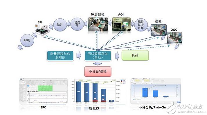
For new process devices, or specially designed devices, suppliers typically offer process control recommendations for temperature profiles and stencil openings. Even if these materials are strictly followed, it is far from producing a satisfactory product. Because of different products, their performance, size, distribution and configuration of the entire board are different; there are differences in equipment and materials from different manufacturers; the acceptable quality, reliability and yield requirements of the final product are also different. the same. All of the above factors require that in the production practice, the field engineer should independently develop and verify the process parameters in addition to carefully setting the process parameters with reference to the materials provided by the supplier. After many accumulations, accurate process data will be obtained.
The following production processes are adjusted and controlled according to the SMT phase control points.
3.1 Chip data
DPS products use a flower ball pad arch chip. The chip name is CORE I7-6600U 2C 4M 2.6G SR2F1 (Figure 2), package size: 42 × 24mm, package is BGA1356.

Figure 2. CORE I7-6600U chip original pad The BGA ball diameter is 0.35mm, but the chip pad design is diversified and the pad shape is different. See Table 1.
3.2 Formulation and implementation plan In combination with the three points of the SMT phase control of the flower ball pad arch chip, the process parameter setting scheme is formulated:
First: adjust the temperature curve to solve the chip deformation problem. The furnace temperature peak reaches 240 degrees or more, and the 12 temperature zone is selected: the reflow furnace, and the temperature rise and temperature drop slopes are controlled at 2-3 ° C / sec;
Second: focus on adjusting the opening method of the stencil. Focus on increasing the amount of solder paste.
This product uses PITCH=0.4mm IC component and 0201 RC component. In order to balance the welding quality of the whole board component, the stencil thickness is 0.12mm stepped stencil, the stencil thickness is 0.12mm steel piece, PITCH=0.4 A 0.10 mm step is used for the IC component of mm and the RC component of 0201. For the four corners and the middle of the easy solder joint position, increase the screen opening under the premise of ensuring the safety distance. In combination with the characteristics of the components of the product, following the principle that the solder joint spacing is not more than 0.2 mm, the opening scheme is as follows (Fig. 3). The specific data is shown in Table 3:
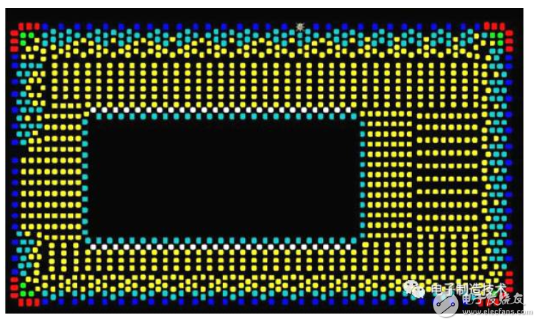
Figure 3, chip pad opening changes according to IPC-7525 steel mesh design guidelines, in order to ensure that the solder paste can be smoothly released from the stencil opening to the PCB pad, in the opening of the stencil, the area ratio > 0.66. The yellow position of the stencil is the smallest, and the calculated area ratio is 0.35*0.35/2*(0.35+0.35)*0.12=0.73>0.67. Therefore, the stencil adopts a steel sheet thickness of 0.12 mm, which can meet the requirements.
Third: solder paste select a brand of high adhesion solder paste, choose No. 4 powder particles. In order to increase the transfer rate of the screen, nano film technology is adopted. At the same time, the stencil time is required to be controlled within 2 hours to ensure flux activity. The product is produced according to the above process scheme, and the BGA and PCB achieve a good fit, forming a good coplanarity; the solder joints produced are in good condition. There are no bridging, solder joint stretching and solder joints. See X-ARY inspection image (Figures 4 and 5). The quality of the later production was stable and there were no quality problems.
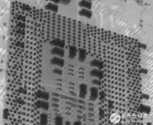
Figure 4, I7-6600U image local
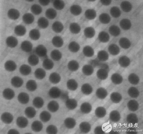
Figure 5, I7-6600U image partial magnification
3.3 Post-Verification Verification 1: When producing SOM products, the same type of chip was found. The chip name is CORE I7-4650U, package size 40mm x 24mm x 1.5mm, FCBGA1168? (see Figure 6, Figure 7). After product review, it is decided to still use the stepped stencil. The thickness of the stencil is 0.1mm steel sheet, and the BGA adopts 0.12mm step. The opening method is used to control the production process of DSP products. After the production, X-RAY inspection did not show the phenomenon of virtual soldering. After functional testing, the product performance is stable.
Figure 6, I7-4650U chip Figure 7, I7-4650U screen verification 2: Production of XTDB products, the product uses Intel C612 25x25mm 836P FCBGA, the pad design is similar, see (Figure 8, Figure 9), the stencil uses the same Opening scheme. There was no soldering failure after soldering.
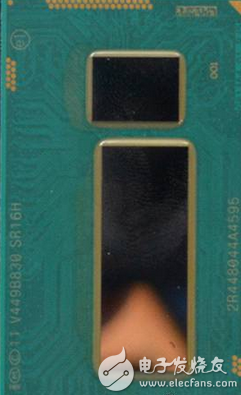
Figure 8, Intel C612 chip

Figure 9. Intel C612 stencil Of course, a stable process parameter is not obtained once, and small details need to be adjusted several times. But the determined process plan is correct and the big direction does not change.
Conclusion In the usual BGA soldering control, solder paste selection and furnace temperature parameter setting are important control aspects of process quality. For the SMT process of the flower ball pad arch chip, in addition to paying attention to the above two aspects of process control, we must also pay attention to the following points:
1) These chips have complex functions. In order to meet the requirements of thinning products, both PCB and BGA are easily deformed. Generally control the furnace temperature curve, need to reach 240 degrees, in order to ensure the BGA leveling, and the PCB flat fit;
2) Expand the stencil opening as much as possible while ensuring that no bridging occurs during the welding process. Under the premise of referring to the stencil opening method recommended by the supplier, the opening change of the solder joint around the four corners of the BGA and the inner ring is mainly considered. By increasing the opening of the stencil, the soldering amount of the solder joint is increased, which can help the flux of the solder paste to maintain activity, and can compensate for the deformation of the solder joint, which is favorable for forming a qualified solder joint;
3) The products using this type of chip are complicated in function, and the types of components used are quite different. In order to ensure the transfer rate of solder paste and avoid bridging, consider the stepped stencil; similarly, the temperature measuring board should pay special attention to various components.
4) Control the stencil time of the solder paste to maintain the activity of the solder paste flux. In combination with the release of the stencil and the selection of tin powder particles, it is considered to use a solder paste with a large adhesive force;
5) During the whole process of SMT, pay attention to ensure that the PCB is well supported or use a suitable tray to avoid deformation.
The analysis of this article is presented to the industry peers, and we look forward to improving our production process quality control capabilities through technical exchanges. Because it is limited to the lack of detection and analysis equipment and my own experience and theoretical level, the deficiencies in the text, experts are welcome to criticize and correct.
Switch Series,Usb Toggle Switch,Double Toggle Switch,Push Button Toggle Switch
Lishui Trimone Electrical Technology Co., Ltd , https://www.3gracegfci.com